Appendix: Hardware Implementation
DG0584 Demo Guide Revision 5.0 27
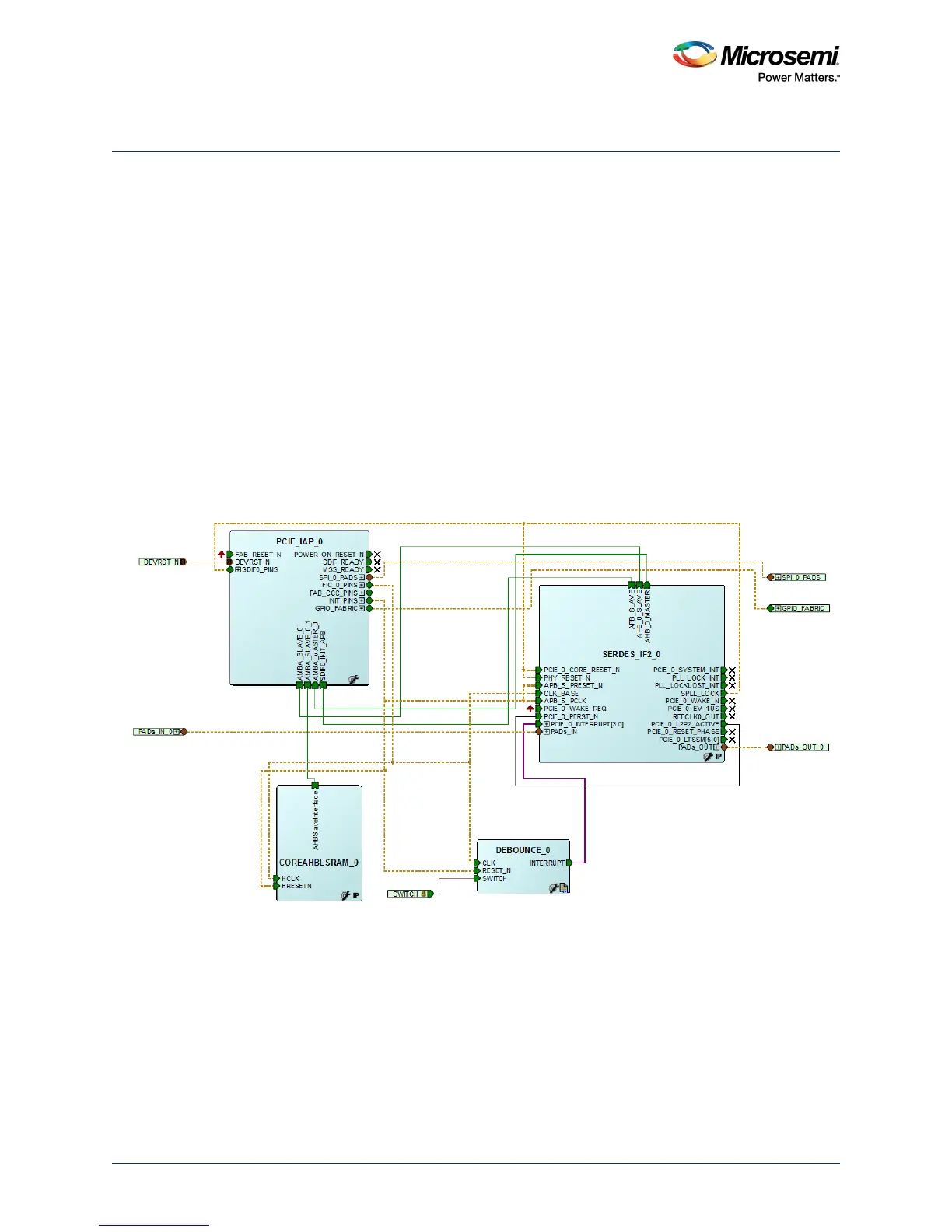
6 Appendix: Hardware Implementation
In this demo design, the following blocks are configured in Libero hardware project:
• The SERDES_IF_1 in the SmartFusion2 device is configured for PCIe 2.0, x4 lanes, and Gen2 rate.
• The CoreAHBLSRAM IP is configured to use the 4 KB of LSRAM.
• The advanced high-performance bus (AHB) master interface of SERDES_IF_1 is enabled and
connected to the AHB slave interface of FIC_0 to access the MSS peripherals. The AHB slave
interface of SERDES_IF_1 and CoreAHBLSRAM IP are connected to the AHB master interface of
FIC_0 to access the PCIe interface and the fabric LSRAM from the MSS.
• BAR0 and BAR1 are configured in the 32-bit memory mapped memory mode. The advanced
extensible interface (AXI) master window 0 is enabled and configured to map the BAR0 memory
address space to the MSS GPIO address space to control the MSS GPIOs. The AXI master window
1 is enabled and configured to map the BAR1 memory address space to the eSRAM address space
to perform read and write operations from the PCIe interface. The AXI slave window 0 is enabled
and configured to map the SmartFusion2 local address space to the host PC address space.
• The MSS GPIO block is enabled and configured: – GPIO_0 to GPIO_7 as outputs and connected to
LEDs – GPIO_8 to GPIO_11 as inputs and connected to DIP switches.
• The M3_CLK clock and Serial Controller 1 clock base are configured to 50 MHz.
• The MSS SPI_0 controller is enabled to access the external SPI Flash memory.
Figure 33 • Demo Design Libero Top-Level Diagram