In-Application Programming Using PCIe Interface
DG0584 Demo Guide Revision 5.0 3
The following figure shows the top-level structure of the design files. For more information, see the
Readme.txt file.
Figure 1 • Demo Design Files Top-Level Structure
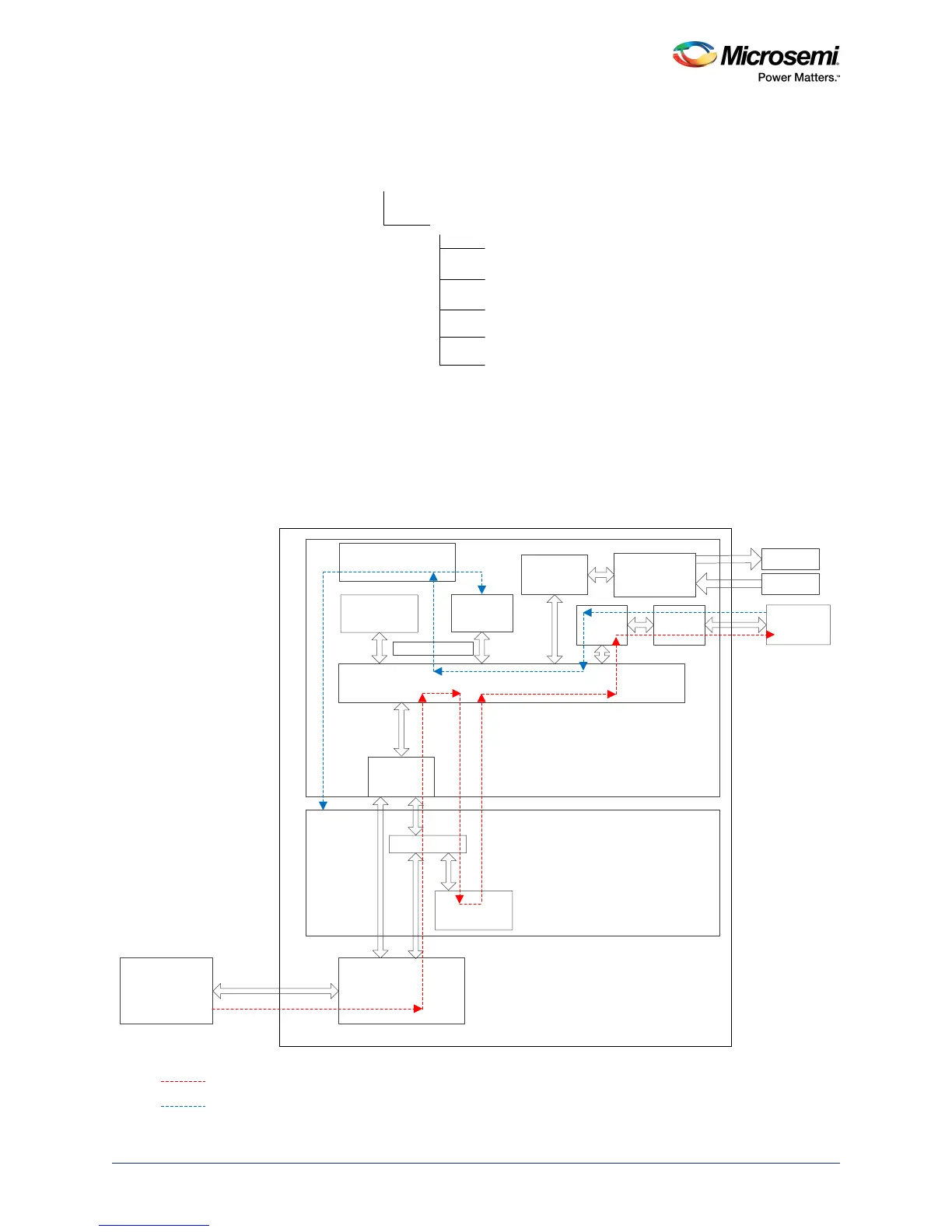
The following figure describes the demo design. The arrows in red show the data flow between the host
PC and the on-board external serial peripheral interface (SPI) flash memory using the PCIe interface.
The ARM
®
Cortex
®
-M3 processor copies the programming data from the host PC to the SPI flash by
using the large static random access memory (LSRAM) memory as a temporary buffer.
The lines in blue show the system controller reading data from the external SPI flash memory to program
the SmartFusion2 device. For more information about IAP process, see Description, page 4.
Figure 2 • Top-Level Demo Block Diagram
<download_folder>
sf2_iap_using_interface_demo_df
libero
pcie_driver
staple_programming_file
sample_programming_files
readme.txt
Serial Controller 0
(PCIe(x4) GEN 2)
FIC_0
AHB Bus Matrix
GPIO
eNVM
APB_1
LEDs
Switches
GUI
Host PC
MSS
SmartFusion2
CoreAHBLite
Cortex – M3
M
S
S
M
APB_0 SPI_0
External
SPI Flash
System Controller
COMM_BLK
Step1
Step2
Transferring data bitstream from host PC to external Flash through PCIe interface
PCIe Interface
System controller reads data bitstream from the external flash to program the SmartFusion2 device
FPGA Fabric
CoreAHB
LSRAM