Appendix: Implementing Workaround to Access Fabric LSRAM after IAP/ISP Program
Operation
DG0584 Demo Guide Revision 5.0 32
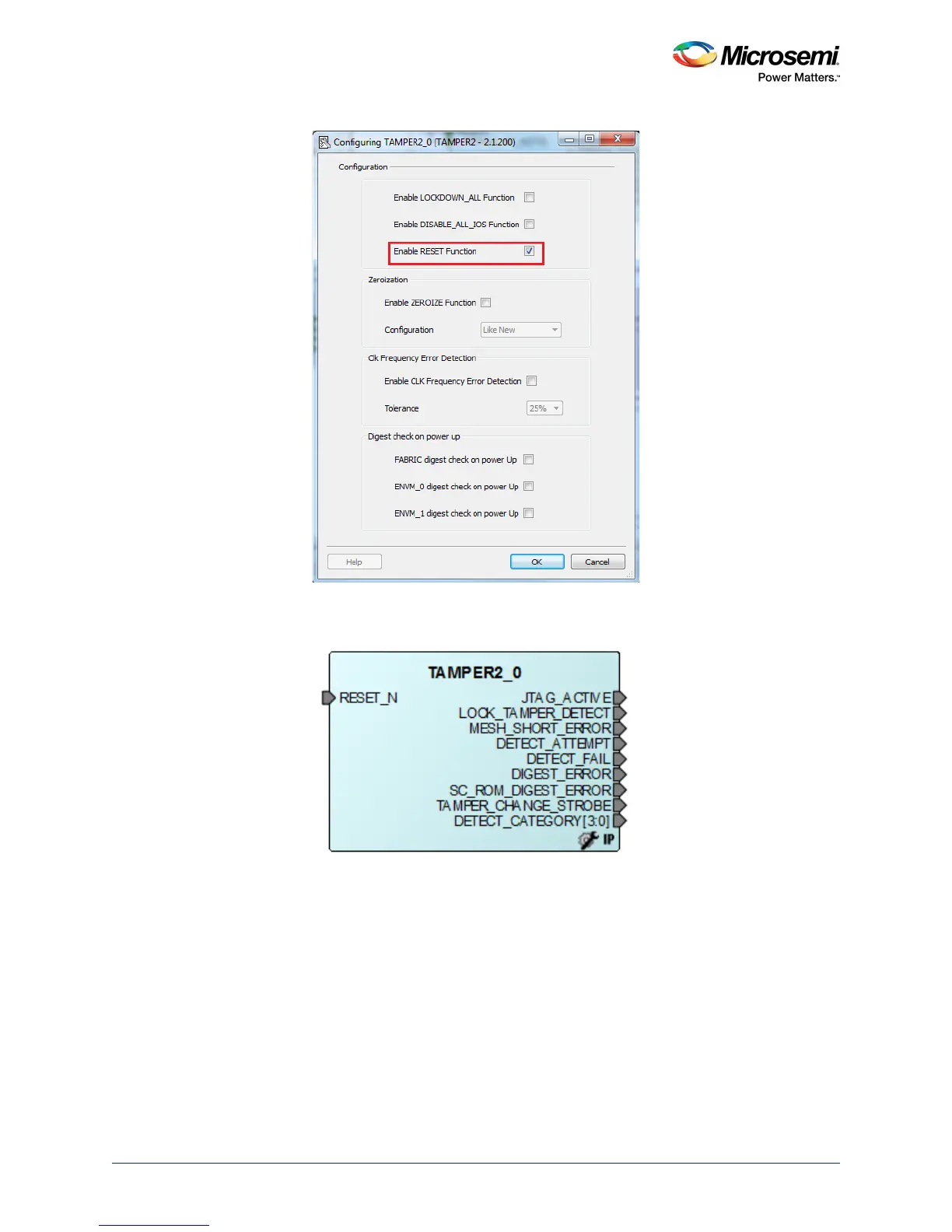
Figure 39 • Tamper Macro Configuration Window
The following figure shows the TAMPER2_0 macro after configuration.
Figure 40 • Tamper Macro - After Configuration
4. Instantiate the FSM Module provided in the design files. This FSM logic performs three consecutive
address writes to the two-port large SRAM with the known data pattern and then reads back data
from those three consecutive address locations to compare. If the read back data pattern does NOT
match the written data pattern, the FSM asserts the RESET_N input to Tamper Macro, which in turn
causes a System Reset. If the read back data pattern matches the written data pattern, the FSM
does not do anything.
Follow these steps to add the FSM logic to the PCIe IAP design:
a. Choose File > Import > HDL Source Files.
b. Browse to the Ram_interface.v file location in the design files folder.
<download_folder>\sf2_iap_using_interface_demo_df\sample_programming_files\LSRAM_Work-
around\Sourcefiles