6 HIGH-SPEED COUNTER MODULE REPLACEMENT
6 - 13
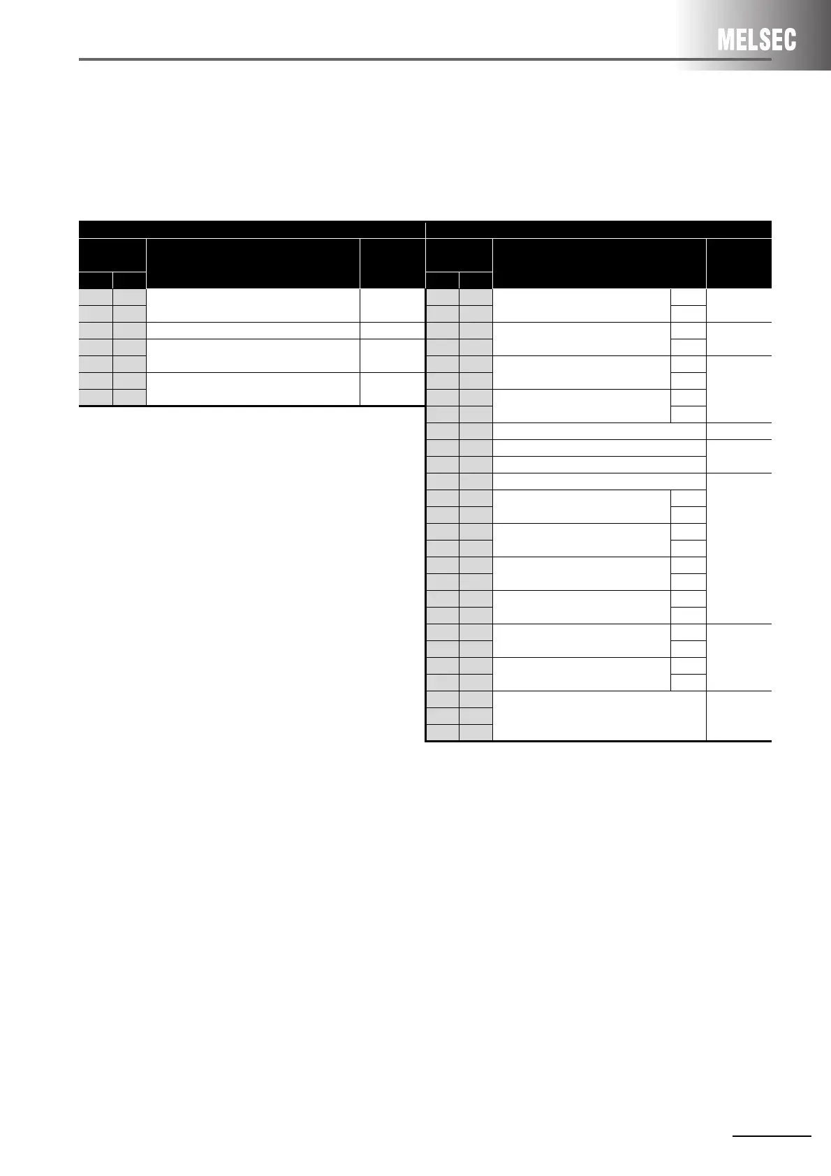
6.3.4 Buffer memory address comparison
Sequence program change is required as the assignment of buffer memory differs.
For details of the buffer memory or sequence program, refer to the High-Speed Counter Module User’s
Manual.
AD61S1 QD62-H02
Address
(Dec.)
Name Read/write
Address
(Dec.)
Name Read/write
CH1 CH2 CH1 CH2
1 33 Preset value write (Lower and middle)
Preset value write (Upper)
W
0 32
Preset value setting
(L)
R/W
(2) (34) 1 33 (H)
3 35 Mode register R/W 2 34
Present value
(L)
R
4 36 Present value read (Lower and middle)
Present value read (Upper)
R
3 35 (H)
(5) (37) 4 36
Coincidence output point set No.1
(L)
R/W
6 38 Set value read/write (Lower and middle)
Set value read/write (Upper)
R/W
5 37 (H)
(7) (39) 6 38
Coincidence output point set No.2
(L)
Address in parentheses in the above table indicates the upper 8 bits
of 24-bit data.
7 39 (H)
8 40 Overflow detection flag R
9 41 Counter function selection setting
R/W
10 42 Sampling/periodic setting
11 43 Sampling/periodic counter flag
R
12 44
Latch count value
(L)
13 45 (H)
14 46
Sampling count value
(L)
15 47 (H)
16 48 Periodic pulse count previous
value
(L)
17 49 (H)
18 50
Periodic pulse count present value
(L)
19 51 (H)
20 52
Ring counter minimum value
(L)
R/W
21 53 (H)
22 54
Ring counter maximum value
(L)
23 55 (H)
24 56
System area (Not used) -to to
31 63
 Loading...