124
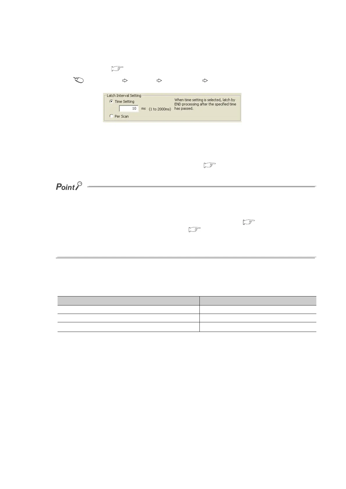
(b) Latch interval setting (High-speed Universal model QCPU and Universal model
Process CPU only)
A latch timing is set. ( Page 446, Appendix 1.2.8)
Project window [Parameter] [PLC Parameter] "Device" tab
(6) Device data latch method and influence on the scan time
Data latch processing is performed during END processing.
For this reason, the scan time increases.
Consider an influence on the scan time when latching devices. ( Page 477, Appendix 3.2 (6))
To minimize the scan time increase due to latch
*1
, reduce the number of latch points (latch (1) setting, latch (2) setting, and
latch relay) as much as possible by performing the following.
• Move latch-target data to the file register.
• Store device data that is less frequently updated in the standard ROM using the SP.DEVST instruction. (The data
stored in the standard ROM can be read using the S(P).DEVLD instruction.) ( Page 258, Section 3.30)
• Set the latch interval parameter to "Time Setting". ( Page 124, Section 3.3 (5) (b))
*1 With the file register (including the extended data register (D) and extended link register (W)), the scan time is not
increased due to latch.
(7) Device data latch clear
The following table lists the status of device data when the latch clear operation is performed.
*1 For the clearing method, refer to Page 75, Section 2.7 (4).
(8) Precautions
(a) When a local device or initial device value is specified
Even data of the latch-specified devices cannot be latched.
(b) Use of battery
Device data in the latch range are held with the battery installed to the CPU module.
• Even for the boot operation, the battery is required to latch device data.
• Note that if the battery connector is disconnected from the connector of the CPU module while the power
supply for the programmable controller is off, device data in the latch range will not be held and will
become undefined.
Latch setting Status of data
Device data without latch setting Cleared
Device data in the "Latch (1)" range Cleared
Device data in the "Latch (2)" range
Held
*1
 Loading...