3 - 13 3 - 13
MELSEC-Q
3 SPECIFICATIONS
3.2.2 Maximum and minimum values hold function
(1) The maximum and minimum values are held in the buffer memory channel by
channel.
(2) The maximum and minimum values are cleared to 0 when the maximum
value/minimum value reset request (YD) or operating condition setting request
(Y9) is turned ON, and new maximum and minimum values are stored when
conversion is started.
(3) Since the area for storing the maximum and minimum values can be rewritten with
the sequence program, the maximum and minimum values within a specific period
of time can be checked.
3.2.3 Input signal error detection function
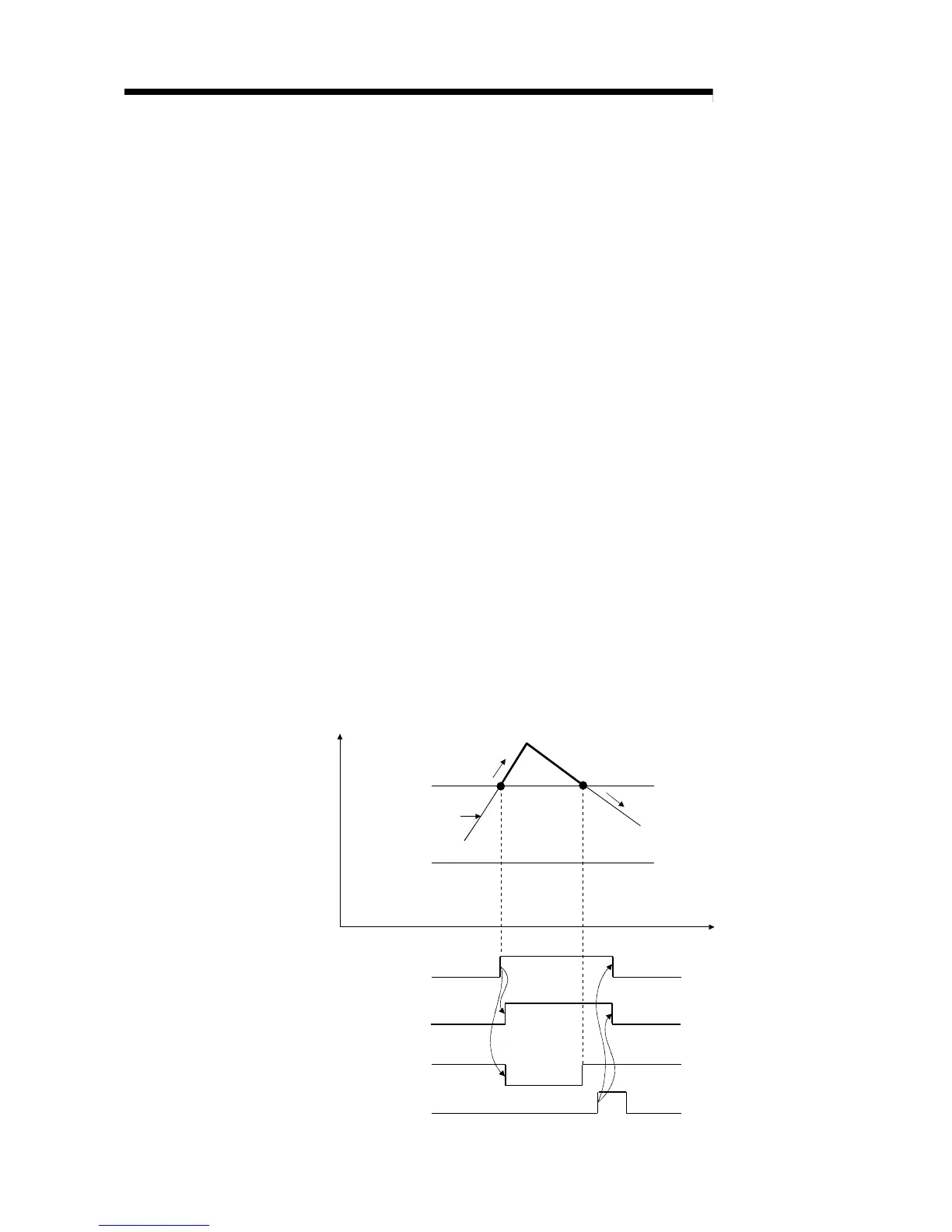
(1) If the input voltage/current rose to or above the input signal error detection upper
limit value or fell to or below the lower limit value, the input signal error detection
flag (buffer memory address 49: Un\G49) and input signal error detection signal
(XC) turn ON and the ALM LED flickers to indicate the error.
(2) The digital output value of the channel where the input signal error detection flag
(buffer memory address 49: Un\G49) turned ON is held as immediately before
detection of the error, and the A/D conversion completed flag (buffer memory
address 10: Un\G10) of the corresponding channel turns OFF.
(3) By bringing the analog input value within the setting range and then turning ON
the error clear request (YF), the input signal error detection flag (buffer memory
address 49: Un\G49) and input signal error detection signal (XC) turn OFF.
(4) When the analog input value returns to within the setting range, A/D conversion is
resumed independently of whether the input signal error detection flag (buffer
memory address 49: Un\G49) and input signal error detection signal (XC) are
reset or not, the A/D conversion completed flag (buffer memory address 10:
Un\G10) of the corresponding channel turns ON again after the first updating.
(The ERR. LED remains flickering.)
Analog input value
Error detection
Upper limit
value
CH1 analog
input value
Lower limit
value
Input value
normal
Time
CH1 input signal error detection flag
(Buffer memory address 49, b0)
Input signal error detection signal (XC)
CH1 A/D conversion completed flag
(Buffer memory address 10, b0)
Error clear request (YF)
 Loading...