717
3
2
3
A
5
6
7
8
Appendix 1OPERATION PROCESSING TIME
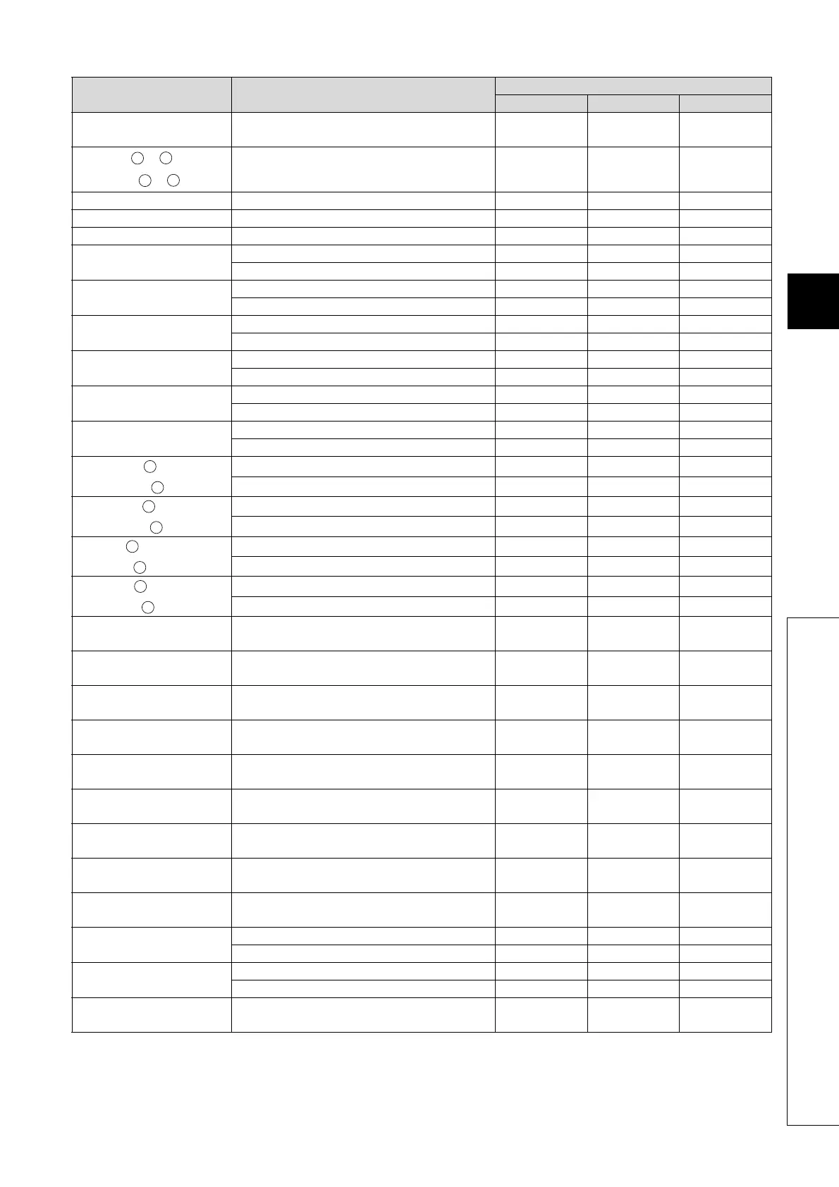
Appendix 1.2Operation Processing Time of Basic Model QCPU
*1: The FROM/TO instruction differs in processing time according to the number of slots and the loaded modules. (The CPU also
differs in processing time according to the extension base type.)
Instruction Condition (Device)
Processing Time (µs)
Q00JCPU Q00CPU Q01CPU
FCALL Pn
FCALLP Pn
–– 29 24 22
FCALL Pn to
FCALLP Pn to
–– 250 205 190
COM –– 110 77 72
IX –– 65 54 51
IXEND –– 302625
IXDEV + IXSET
Number of contacts 1 145 120 110
Number of contacts 14 770 630 585
FIFW
FIFWP
Number of data points 0 36 32 28
Number of data points 96 36 32 28
FIFR
FIFRP
Number of data points 1 45 41 36
Number of data points 96 93 82 70
FPOP
FPOPP
Number of data points 1 40 37 32
Number of data points 96 40 37 32
FINS
FINSP
Number of data points 0 53 44 38
Number of data points 96 100 89 76
FDEL
FDELP
Number of data points 1 60 50 43
Number of data points 96 110 95 82
FROM n1 n2 n3
FROMP n1 n2 n3
*1
n3 = 1 125 105 93
n3 = 1000 740 695 685
DFRO n1 n2 n3
DFROP n1 n2 n3
*1
n3 = 1 130 110 100
n3 = 500 745 695 675
TO n1 n2 n3
TOP n1 n2 n3
*1
n3 = 1 120 105 92
n3 = 1000 735 680 645
DTO n1 n2 n3
DTOP n1 n2 n3
*1
n3 = 1 130 110 99
n3 = 500 740 680 640
LIMIT
LIMITP
–– 34 28 26
DLIMIT
DLIMITP
–– 41 34 30
BAND
BANDP
–– 33 28 25
DBAND
DBANDP
–– 40 34 30
ZONE
ZONEP
–– 31 25 24
DZONE
DZONEP
–– 37 29 28
RSET
RSETP
–– –– 18 16
DATERD
DATERDP
–– 30 25 23
DATEWR
DATEWRP
–– 69 57 54
DATE+
DATE+P
No digit increase 47 39 36
Digit increase 50 42 38
DATE -
DATE - P
No digit increase 47 40 36
Digit increase 50 42 38
SECOND
SECONDP
–– 28 24 22
S1
S5
S1
S5
D
D
D
D
S
S
S
S
 Loading...