777
3
2
3
A
5
6
7
8
Appendix 1OPERATION PROCESSING TIME
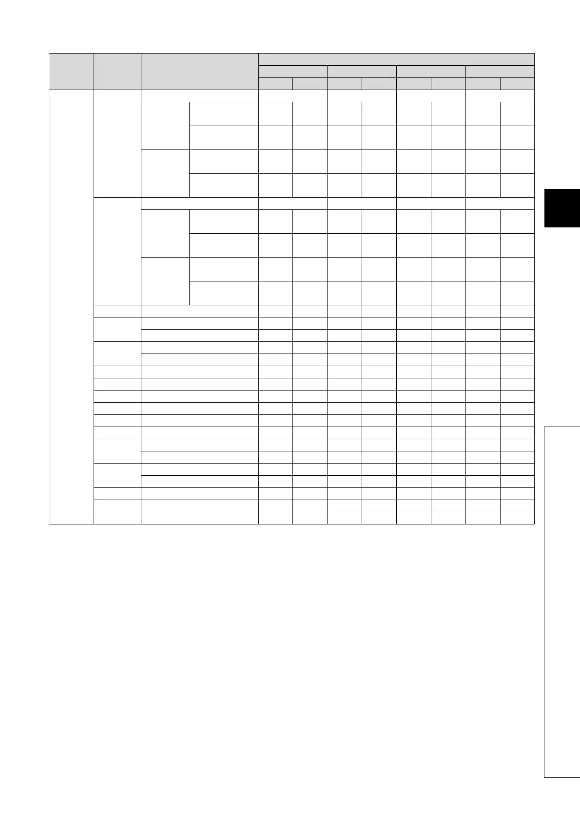
Appendix 1.4Operation Processing Time of Universal Model QCPU
Category Instruction Condition (Device)
Processing Time (µs)
Q00UJCPU Q00UCPU Q01UCPU Q02UCPU
Min. Max. Min. Max. Min. Max. Min. Max.
Application
instruction
ANDTM>=
When not executed
0.480 0.320 0.240 0.160
Comparison
of specified
clock
In conductive
status
8.200 25.500 8.200 25.500 6.500 25.500 7.000 23.000
In non-conductive
status
8.200 25.500 8.200 25.500 6.500 25.500 7.000 23.000
Comparison
of current
clock
In conductive
status
6.500 23.100 6.500 23.100 6.500 23.100 5.600 21.900
In non-conductive
status
6.500 23.100 6.500 23.100 6.500 23.100 5.600 21.900
ORTM>=
When not executed
0.480 0.320 0.240 0.160
Comparison
of specified
clock
In conductive
status
8.200 25.500 8.200 25.500 6.500 25.500 7.000 23.000
In non-conductive
status
8.200 25.500 8.200 25.500 6.500 25.500 7.000 23.000
Comparison
of current
clock
In conductive
status
6.500 23.100 6.500 23.100 6.500 23.100 5.900 22.100
In non-conductive
status
6.500 23.100 6.500 23.100 6.500 23.100 5.900 22.100
S.DATERD ––
9.250 51.000 9.250 51.000 9.250 51.000 7.500 23.400
S.DATE +
No digit increase
16.800 75.400 16.800 75.400 16.800 75.400 9.100 23.400
Digit increase
16.800 75.400 16.800 75.400 16.800 75.400 8.900 22.200
S.DATE -
No digit increase
17.600 75.300 17.600 75.300 17.600 75.300 9.000 22.200
Digit increase
16.900 75.300 16.900 75.300 16.900 75.300 9.800 22.100
PSTOP ––
82.200 199.000 82.200 199.000 82.200 199.000 61.400 84.500
POFF ––
82.600 198.000 82.600 198.000 82.600 198.000 121.000 246.000
PSCAN ––
83.600 200.000 83.600 200.000 83.600 200.000 126.000 232.000
WDT ––
2.900 12.000 2.900 12.000 2.900 12.000 1.300 3.000
DUTY ––
7.700 27.500 7.700 27.500 7.700 27.500 4.900 24.300
TIMCHK ––
5.350 24.500 5.350 24.500 5.350 24.500 7.400 23.300
ZRRDB
File register of standard RAM
4.100 4.200 4.100 4.200 4.100 4.200 2.400 2.600
File register of SRAM card
–– –– –– –– –– –– 2.500 2.800
ZRWRB
File register of standard RAM
5.400 5.500 5.400 5.500 5.400 5.500 3.100 3.300
File register of SRAM card
–– –– –– –– –– –– 3.300 3.600
ADRSET ––
2.400 6.650 2.400 6.650 2.400 6.650 4.200 4.900
ZPUSH ––
9.200 20.500 9.200 20.500 9.200 20.500 6.900 14.000
ZPOP ––
9.000 15.500 9.000 15.500 9.000 15.500 7.500 12.500
 Loading...