SECTION 5
TIMER
The following paragraphs describe the timer circuitry for the eight versions
of
the M6805 Family
found
in
this document. Note that while each timer consists
of
an
8-bit software programmable
counter driven by a 7-bit prescaler there are three distinctly different configurations (Figures 5-1,
5-2, and 5-3).
5.1
MC6805R2/MC6805U2 TIMER CIRCUITRY
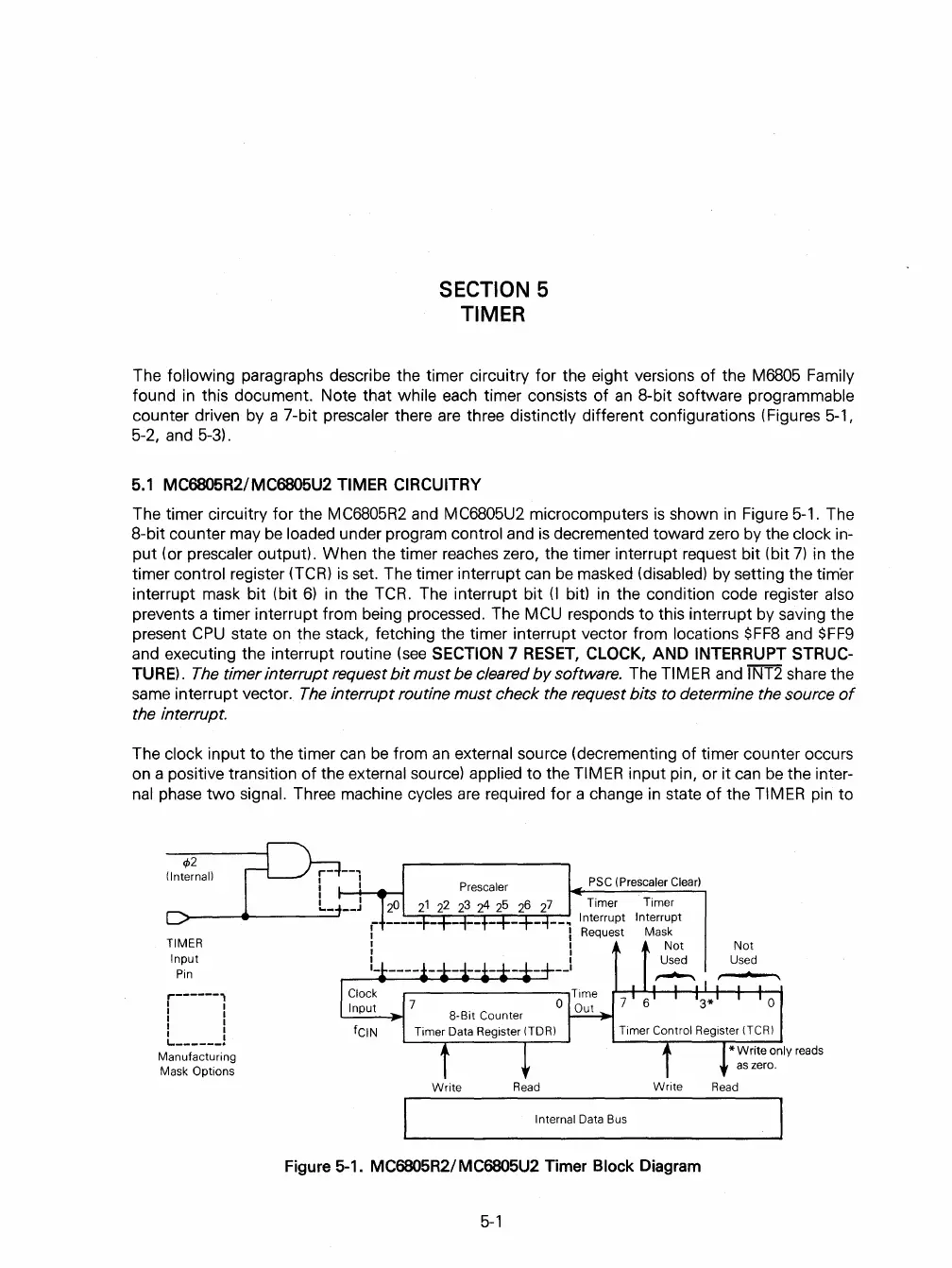
The timer circuitry for the MC6805R2 and MC6805U2 microcomputers
is
shown
in
Figure
5-1.
The
8-bit counter may
be
loaded under program control and
is
decremented toward zero by the clock in-
put
(or prescaler output). When the timer reaches zero, the timer interrupt request bit (bit
7)
in
the
timer
control register (TCR)
is
set. The timer interrupt
can
be
masked (disabled) by setting the timer
interrupt mask bit (bit
6)
in
the TCR. The interrupt bit
(I
bit)
in
the condition code register also
prevents a timer interrupt from being processed. The MCU responds to this interrupt by saving the
present
CPU
state on the stack, fetching the timer interrupt vector from locations
$FF8
and
$FF9
and executing the interrupt routine
(see
SECTION 7
RESET,
CLOCK, AND INTERRUPT STRUC-
TURE).
The
timer interrupt request
bit
must
be cleared
by
software. The
TI
M
ER
and I NT2 share the
same interrupt vector.
The
interrupt routine
must
check the request bits
to
determine the source
of
the interrupt.
The
clock input to the timer
can
be
from
an
external source (decrementing of timer counter occurs
on a positive transition
of
the external source) applied to the TIMER input pin, or it
can
be
the inter-
nal phase
two
signal. Three machine cycles
are
required for a change
in
state
of
the TIMER pin to
t/>2
(Internal)
TIMER
Input
Pin
r------1
I I
I I
I I
I I
I I
1...
______
•
Manufacturing
Mask
Options
Write
Read
PSC
(Prescaler
Clear)
Timer Timer
Interrupt
Mask
Not
Write
Internal Data Bus
Figure 5-1. MC6805R2/ MC6805U2 Timer Block Diagram
5-1
Not
Used
o
*
Write
only reads
as
zero.
Read
 Loading...

