SECTION 8
INPUT/OUTPUT CIRCUITRY
AND
ANALOG-TO-DIGITAL CONVERTER
8.1
INPUT/OUTPUT CIRCUITRY
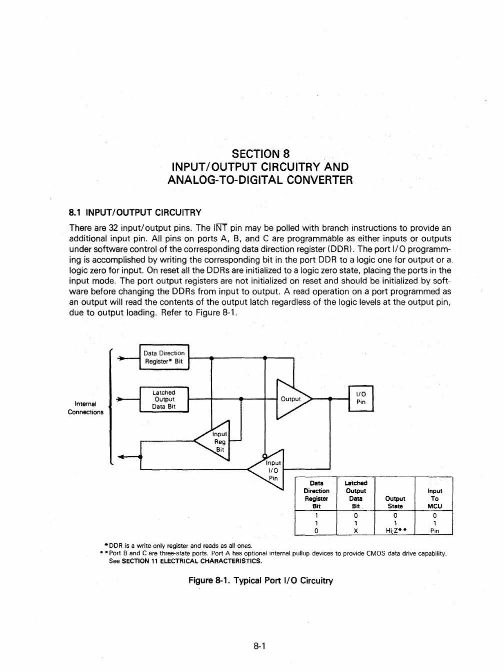
There
are
32
input/
output pins. The INT pin may
be
polled with branch instructions
to
provide
an
additional input pin. All pins
on
ports A,
B,
and C
are
programmable
as
either inputs or outputs
under software
control of the corresponding data direction register (DDR)' The port
I/O
programm-
ing
is
accomplished by writing the corresponding bit
in
the port
DDR
to a logic one for output or a
logic zero for input.
On
reset
all
the DDRs
are
initialized
to
a logic zero state, placing the ports
in
the
input mode. The port output registers
are
not initialized
on
reset and should
be
initialized by soft-
ware before changing the DDRs from input to output. A
read
operation
on
a port programmed
as
an
output will
read
the contents of the output latch regardless of
the
logic levels at the output pin,
due
to
output loading. Refer to Figure 8-1.
Internal
Connections
* DDR
is
a write-only register and reads
as
all ones.
Data
Direction
Register
Bit
,
,
0
Latched
Output
Data
Bit
0
,
X
Input
Output
To
State MCU
0
0
, ,
Hi~Z*
*
Pin
* * Port
Band
C are three-state ports. Port A
has
optional internal pullup devices to provide CMOS data drive capability.
See SECTION
11
ELECTRICAL CHARACTERISTICS.
Figu
re
8-1. Typical Port
I/O
Circu itry
8-1
 Loading...

