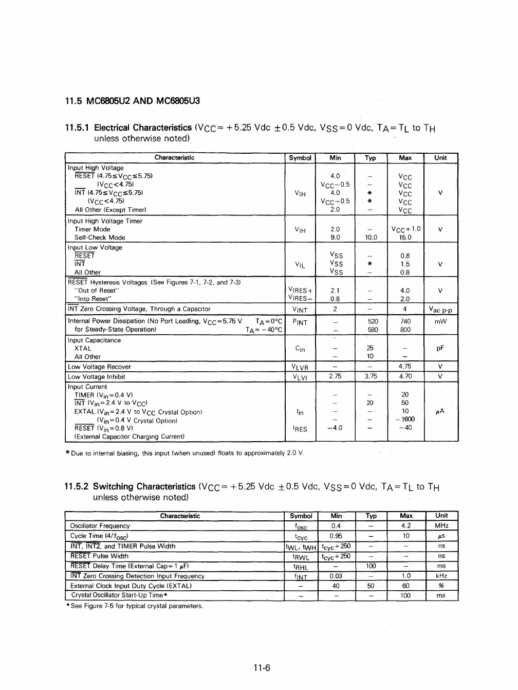
11.5 MC6805U2
AND
MC6805U3
11.5.1 Electrical Characteristics (VCC=
+5.25
Vdc ±O.5 Vdc,
VSS=O
Vdc,
TA=TL
to
TH
unless otherwise noted)
Characteristic
Symbol
Min
Typ
Max
Unit
Input High Voltage
RESET
(4.75SVCCs5.75)
4.0
-
VCC
(VCC<4.75)
VCC-0.5
-
VCC
INT
(4.75sVCCs5.75)
VIH
4.0
*
VCC
V
(VCC<4.75)
VCC-0.5
*
VCC
All Other (Except Timer)
2.0
-
VCC
Input High Voltage Timer
Timer Mode
VIH
2.0
-
VCC+
1.0
V
Self-Check Mode 9.0 10.0
15.0
Input
Low Voltage
RESET
VSS
-
O.S
INT
VIL
VSS
*
1.5
V
All Other
VSS
-
O.S
RESET
Hysteresis Voltages (See Figures 7-1, 7-2, and
7-3)
"Out
of
Reset" VIRES+
2.1
-
4.0 V
"Into
Reset"
VIRES-
O.S
-
2.0
INT
Zero Crossing Voltage, Through a Capacitor
VINT
2
-
4
Vac p-p
Internal Power Dissipation (No Port Loading, V
CC
= 5.75 V
TA=O°C
PINT
-
520
740
mW
for Steady-State Operation)
TA=
-40°C
-
5S0
SOO
Input Capacitance
XTAL
Cin
-
25
-
pF
All Other
-
10
-
Low Voltage Recover
VLVR
- - 4.75
V
Low Voltage
Inhibit
VLVI
2.75
3.75
4.70
V
Input Current
TIMER (Vin=Oo4
V)
-
-
20
INT
(Vin=2.4
V to
VCC)
-
20
50
EXTAL (Vin=204 V to
VCC
Crystal Option)
lin
-
-
10
p.A
__
(Vin=Oo4 V Crystal Option)
- -
-1600
RESET
(Vin=O.S
V)
IRES
~4.0
-
-40
(External Capacitor Charging Current)
*"
Due to internal biasing, this input (when unused) floats to approximately 2.0
V.
11.5.2 Switching Characteristics (VCC=
+5.25
Vdc ±O.5 Vdc,
VSS=O
Vdc,
TA=TL
to
TH
unless otherwise noted)
Characteristic Symbol Min
Typ Max
Unit
Oscillator Frequency
fosc
004
- 4.2
MHz
Cycle Time (4/fos
c
)
tcyc
0.95
-
10
p's
INT, INT2, and TIMER Pulse
Width
tWL, tWH
t
cyc
+250
-
-
ns
RESET
Pulse Width
tRWL
t
cyc
+250
-
-
ns
iiESET Delay Time (External
Cap=
1
p.F)
tRHL
-
100
- ms
iNT
Zero Crossing Detection Input Frequency
flNT
0.03
-
1.0
kHz
External
Clock Input Duty Cycle (EXTAU -
40
50
60
%
Crystal Oscillator Start-Up
Time*
-
- -
100
ms
*
See
Figure 7-5 for typical crystal parameters.
11-6
 Loading...

