b5,
CLS
Timerl Prescaler Clock Source
1 = External
TIMER pin.
0=
Intenal phase two.
b4
Not used if
MOR
TOPT = 1 (MC6805R2/MC6805U2 emulationl. Sets initial value
of
TCR
TIE
if
MOR
TOPT=O (MC6805R3/MC6805U3 emulationl.
b3,
SNM* When this bit
is
set, i.e., programmed to a one, it
is
not possible to access the
EPROM
contents
of
the MC68705R5 and MC68705U5 externally. For more information refer to
9.4 PROGRAMMING FIRMWARE.
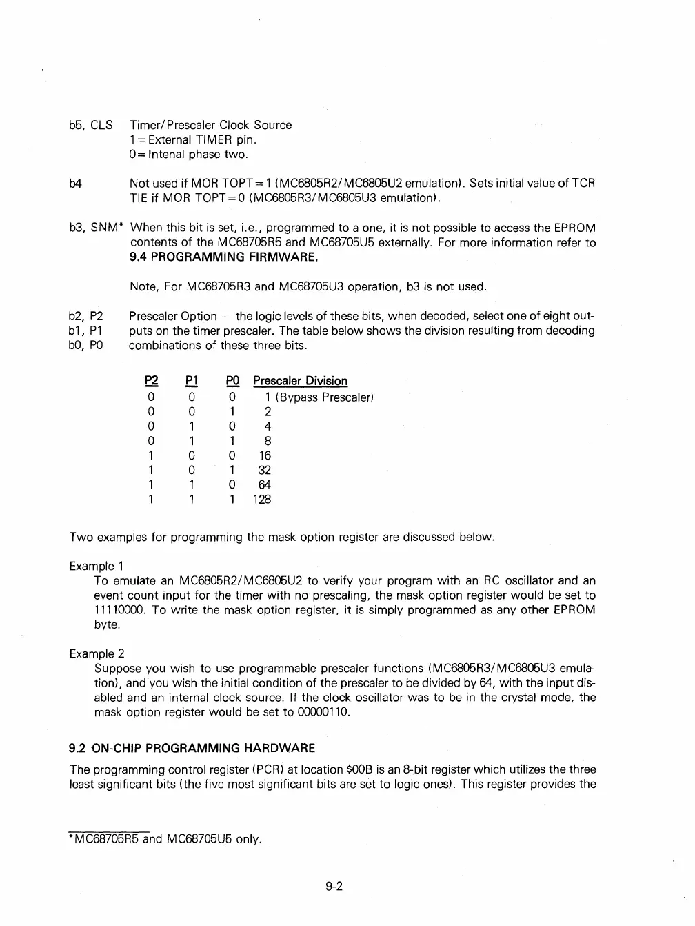
b2,
P2
b1,
P1
bO,
PO
Note, For MC68705R3
and
MC68705U3 operation,
b3
is
not used.
Prescaler
Option - the logic levels
of
these bits, when decoded, select one
of
eight out-
puts
on
the timer prescaler. The table below shows the division resulting from decoding
combinations of these three bits.
P2
Pl
PO
Prescaler
Division
0
0 0
1 (Bypass Prescaler)
0
0
1
2
0 1
0 4
0
1
1
8
1
0
0
16
1
0
1
32
1 1 0
64
1
1
1
128
Two examples for programming the
mask
option register
are
discussed below.
Example 1
To emulate
an
MC6805R2/MC6805U2 to verify your program with
an
RC
oscillator and
an
event count input for the timer with no prescaling, the
mask
option register would
be
set to
11110000.
To write the
mask
option register, it
is
simply programmed
as
any other
EPROM
byte.
Example 2
Suppose you wish to
use
programmable prescaler functions (MC6805R3/MC6805U3 emula-
tion), and you wish the initial condition
of
the prescaler to
be
divided by
64,
with the input dis-
abled and
an
internal clock source. If the clock oscillator was to
be
in
the crystal mode, the
mask
option register would
be
set to
00000110.
9.2 ON-CHIP PROGRAMMING HARDWARE
The programming control register
(PCR)
at location
$OOB
is
an
8-bit register which utilizes the three
least significant bits (the five most significant bits
are
set
to
logic ones). This register provides the
*MC68705R5
and
MC68705U5 only.
9-2
 Loading...

