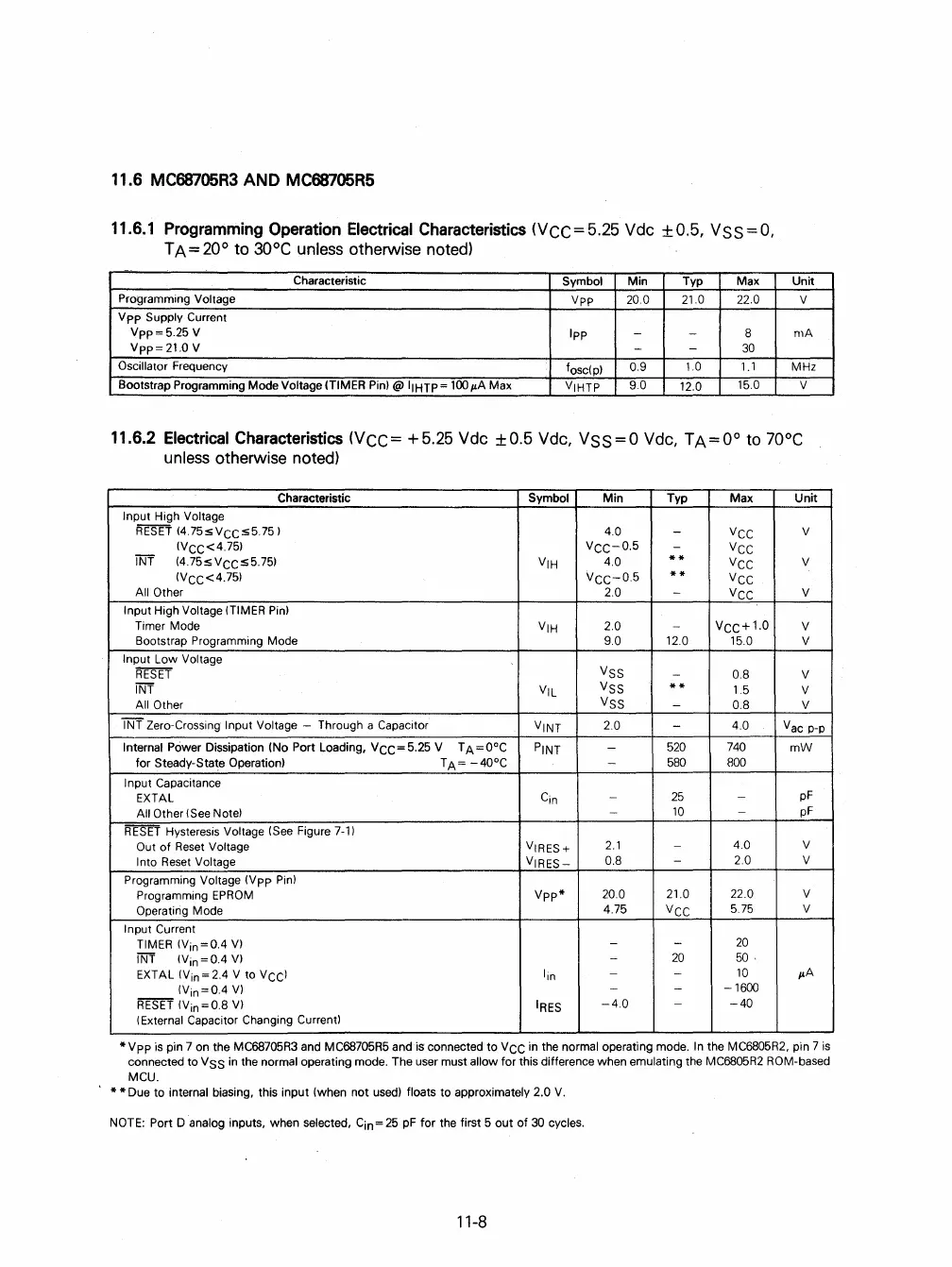
11.6
MC68705R3
AND
MC68705R5
11.6.1
Programming
Operation
Electrical
Characteristics
(Vee=5.25
Vdc
±0.5,
VSS=O,
T A = 20° to
30
0
e unless otherwise noted)
Characteristic
Symbol Min
Typ
Max
Programming Voltage
VPP
20.0 21.0 22.0
VPP
Supply Current
Vpp=5.25
V
Ipp
-
-
8
Vpp=21.0
V - -
30
Oscillator Frequency
fos
c
(p)
0.9
1.0
1.1
Bootstrap Programming Mode Voltage (TIMER Pin) @ IIHTP =
100
p.A
Max
VIHTP
9.0
12.0
15.0
Unit
V
mA
MHz
V
11.6.2
Electrical
Characteristics
(Vee=
+5.25 Vdc
±0.5
Vdc, VSS=O Vdc,
TA=O°
to
70
0
e
unless
otherwise noted)
Characteristic Symbol Min Typ
Max
Unit
Input High Voltage
R'ESTI
(4.75sVCCs5.75)
4.0
-
VCC
V
(VCC<4.75)
VCC-0.5
-
VCC
INT
(4.75 s V
CC
s 5.75)
VIH
4.0
**
VCC
V
(VCC<4.75)
VCC-0.5
**
VCC
All Other 2.0
-
VCC
V
Input
High Voltage (TIMER
Pin)
Timer Mode
VIH
2.0
-
VCC+
1.0
V
Bootstrap Programming Mode 9.0 12.0 15.0
V
Input
Low Voltage
RESET
VSS
-
0.8 V
INT
VIL
VSS
**
1.5
V
All Other
VSS
-
0.8 V
INT Zero-Crossing Input Voltage
- Through a Capacitor
VI
NT
2.0
-
4.0
Vac
p-p
Internal Power Dissipation (No Port Loading.
VCC=5.25
V
TA=O°C
PINT
-
520
740
mW
for Steady-State Operation)
TA=-40°C
-
580
800
Input Capacitance
EXTAL
Cin
-
25
-
pF
All Other (See Note)
-
10
-
pF
RESET
Hysteresis Voltage (See Figure 7-1)
Out
of
Reset Voltage
VIRES+
2.1
-
4.0 V
Into
Reset Voltage
VIRES-
0.8
- 2.0 V
Programming Voltage
(Vpp
Pin)
Programming
EPROM
Vpp*
20.0
21.0 22.0 V
Operating Mode
4.75
VCC
5.75
V
Input Current
TIMER (Vin
= 0.4
V)
-
-
20
INT
(Vin=OA
V)
-
20
50
.
EXT
AL (Vin = 2.4 V to V
CC)
lin
-
-
10
p.A
(Vin=O.4
V)
- -
-1600
RESET
(Vin = 0.8
V)
IRES
-4.0
-
-40
(External Capacitor Changing Current)
*
Vpp
is
pin 7 on the MC68705R3 and MC68705R5 and is connected
to
VCC
in the normal operating mode.
In
the MC6805R2, pin 7
is
connected
to
VSS in the normal operating mode. The user must allow for this difference when emulating the MC6805R2 ROM-based
MCU.
*
*Due
to internal biasing. this input (when not used) floats
to
approximately 2.0
V.
NOTE: Port D analog inputs. when selected.
Cin=25
pF
for
the first 5
out
of
30 cycles.
11-8
 Loading...

