necessary control bits
to
allow programming the EPROM. The bootstrap program manipulates the
PCR
when programming
so
that users
need
not
be
concerned
with
the
PCR
in
most applications. A
description
of
each
bit follows.
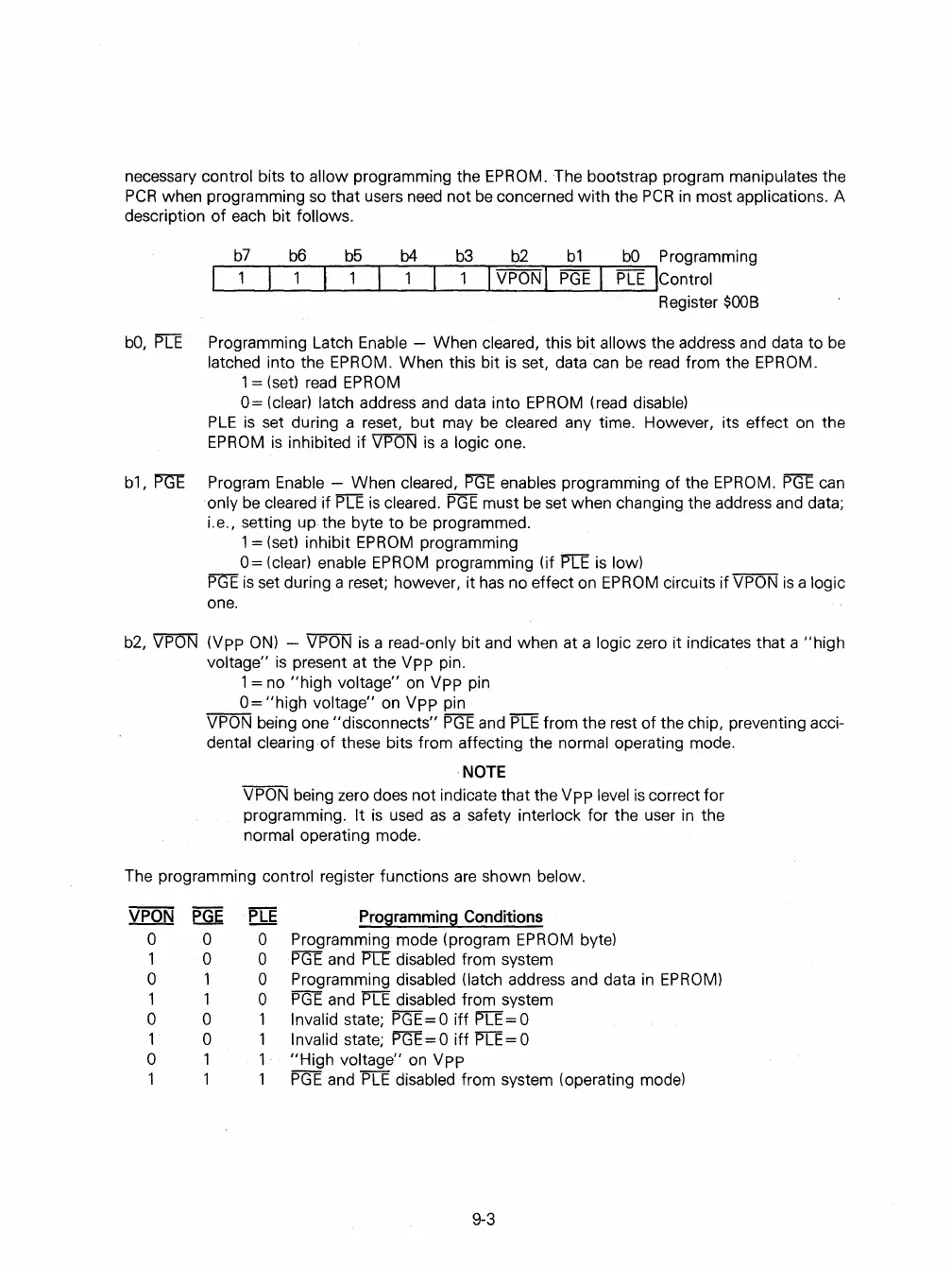
b7
b6 b5
b4
b3
b2
b1
bO
Programming
I VPON I
PGE
I
PLE
IControl
Register $008
bO,
PIE
Programming Latch Enable - When cleared, this bit allows the address and data to
be
latched into the EPROM. When this bit
is
set, data can
be
read
from the EPROM.
1 = (set)
read
EPROM
0=
(clear) latch address and data into
EPROM
(read disable)
PLE
is
set during a reset, but may
be
cleared any time. However, its effect on the
EPROM
is
inhibited if VPON
is
a logic one.
b1,
J5GE
Program Enable - When cleared,
f5GE
enables programming
of
the EPROM.
PGE
can
only
be
cleared if PIT
is
cleared.
PGE
must
be
set when changing the address and data;
i.e., setting up the byte
to
be
programmed.
1 = (set) inhibit
EPROM
programming
0=
(clear) enable
EPROM
programming (if
PIE
is
low)
PGE
is
set during a reset; however, it
has
no effect on
EPROM
circuits if VPON
is
a logic
one.
b2,
VPON (Vpp
ON)
- VPON
is
a read-only bit and when at a logic zero it indicates that a
"high
voltage"
is
present at the
Vpp
pin.
1 = no
"high
voltage" on
Vpp
pin
0=
"high
voltage" on
Vpp
pin
VPON being one "disconnects"
PGE
and
PLE
from the rest
of
the chip, preventing acci-
dental clearing
of
these bits from affecting the normal operating mode .
. NOTE
VPON being zero does not indicate that the
Vpp
level
is
correct for
programming.
It
is
used
as
a safety interlock for the user
in
the
normal operating mode.
The programming
control register functions
are
shown below.
VPON
PGE
PLE
Programming Conditions
a a a Programming mode (program
EPROM
byte)
1 a
o
PG
E and
PLE
disabled from system
a 1 a Programming disabled (latch address and data
in
EPROM)
1 1
a
PG
E and
'PIE
disabled from system
a a
1 Invalid state; PGE=O iff
PIT
= a
1 a 1 Invalid state; PGE=O
iff
PIT = a
a
1
"High
voltage" on
Vpp
1
1
PGE
and
PLE
disabled from system (operating mode)
9-3
 Loading...

