All
inputloutput
lines
are
TTL compatible
as
both inputs and outputs. Port A lines
are
CMOS com-
patible
as
outputs (mask option on the MC6805R2, MC6805U2, MC6805R3, and MC6805U3) while
port
B,
C,
and 0 lines are CMOS compatible
as
inputs. Port 0 lines are input only; thus, there
is
no
corresponding DDR. When programmed
as
outputs, port b
is
capable of sinking
10
milliamperes
and sourcing 1 milliampere on each pin.
Port
0 provides the reference voltage, INT2, and multiplexed analog inputs for the MC6805R2,
MC6805R3, MC68705R3,
and MC68705R5. All
of
these lines
are
shared with the port 0 digital in-
puts. Port
0 may always
be
used
as
digital inputs and may also
be
used
as
analog inputs providing
VRH
and
VRl
are connected to the appropriate reference voltages.
TheVRl
and VRH lines (PD4
and
PD5)
are
internally connected
to
the
AID
resistor. Analog inputs may
be
prescaled to attain the
VRl
and
VRH
recommended input voltage range.
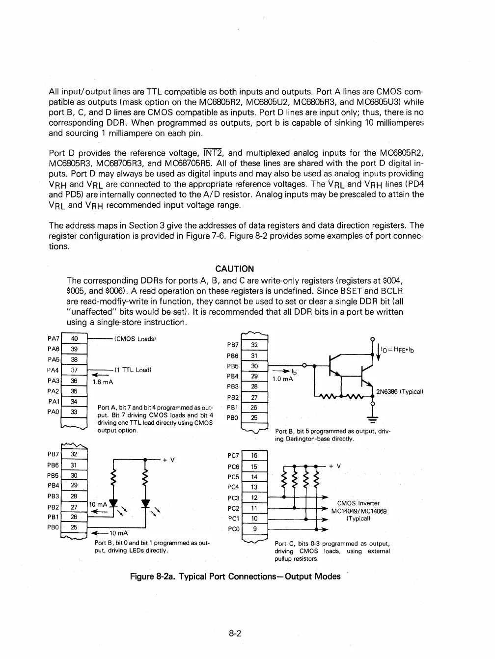
The address maps
in
Section 3 give the addresses
of
data registers and data direction registers. The
register configuration
is
provided
in
Figure 7-6. Figure 8-2 provides some examples
of
port connec-
tions.
CAUTION
The corresponding DDRs for ports A,
B,
and C are write-only registers (registers at
$004,
$005,
and
$006),
A
read
operation on these registers
is
undefined. Since BSET and
BClR
are read-modfiy-write
in
function, they cannot
be
used
to
set or clear a single
DDR
bit (all
"unaffected"
bits would
be
set).
It
is
recommended that
all
DDR
bits
in
a port
be
written
using a
single-store instruction.
PA7
40
(CMOS Loads)
PA6
PA5
PA2
PAl
PAO
PB7
PB6
PB5
PB3
PB2
PBl
PBO
(1
TTL Load)
Port A, bit 7
and
bit 4 programmed
as
out-
put. Bit 7 driving
CMOS loads and bit 4
driving
one
TTL load directly using CMOS
output option.
10mA
~.
.--~.....--+
V
~10mA
Port B, bit 0
and
bit 1 programmed
as
out-
put, driving
LEOs
directly.
PB7
32
PB6
31
PB5
30
PB4
29
PB3
28
PB2
27
PBl
26
PBO
25
PC7
16
PC6
15
PC5
14
PC4
13
PC3
12
PC2
11
PCl
10
PCO
9
-'Ib
1.0
mA
~""'''''''JV'''''--'
2N6386 (Typical)
Port
B,
bit 5 programmed
as
output, driv-
ing Darlington-base directly.
CMOS Inverter
MCl4049/MCl4069
(Typical)
Port
C,
bits
0-3
programmed
as
output,
driving
CMOS loads, using external
pullup resistors.
Figure 8-2a. Typical Port
Connections-
Output Modes
8-2
 Loading...

