VS1 Operations and Maintenance Manual Description
Issue 3.1 2013-10-01 Page 1-1
Section 1: Description
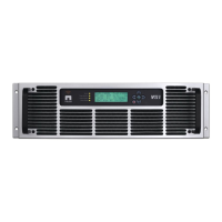
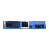
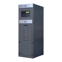
Refer to the functional block diagram: Block Diagram - VS1 Transmitter - see page 1-7.
This section provides a high-level description of the transmitter’s key sections. The transmitter
circuitry is subdivided into four basic stages:
• Ac-dc power stage
• Exciter/control stage - see page 1-3
• RF drive stage - see page 1-4
• RF power stage - see page 1-4
VS1 electrical schematics
Some descriptions in this section refer to electrical schematics (SD-#s) . These are located in
Section 5 of the VS1 Troubleshooting Manual.
Ac-dc power stage
See also electrical schematic Figure SD-1.
The ac-dc power stage converts the ac power source to a positive dc voltage (PA volts) for the
transmitter's PA PWBs. The transmitter accepts a 1-phase ac input voltage that is between 180 and
264 V ac (208 V ac nominal).
The ac-dc power stage provides +48 V to operate the RF power stage’s pre-amp/IPA PWB, as well
as the cooling fans and the low level dc voltages (+15 V and +5 V) for the control/monitoring
circuitry used throughout the transmitter.
The ac-dc power stage consists of ac power entrance U1, circuit breaker CB1, power supply module
U2, +48 V power supply module U3 and PS distribution PWB A2.