⚫
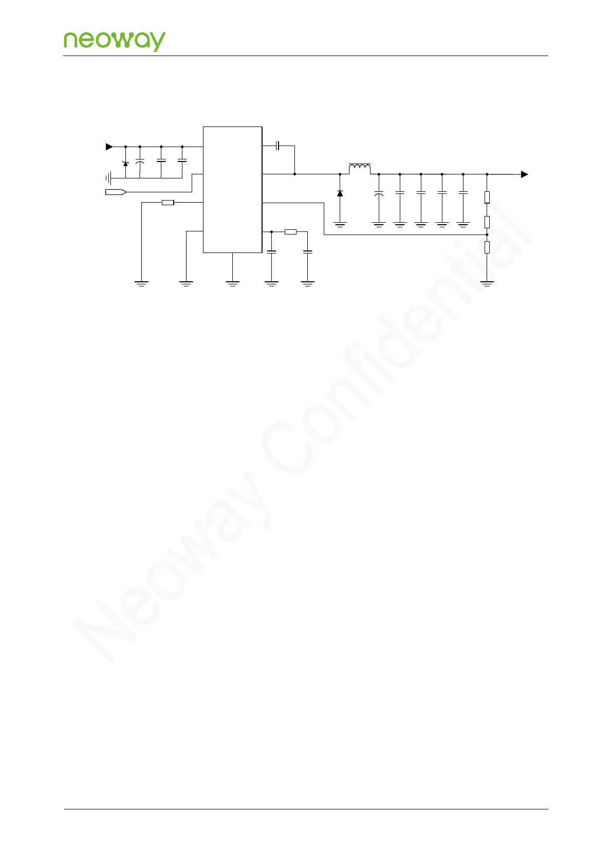
As there is a big difference between the power input and VBAT, the DC-DC step-down chip
should be selected, and the maximum output current should be at least 2.5 A.
⚫
Place the TVS (D2) close to the power input interface to clamp the surge voltage before it enters
back-end circuits to ensure that the back-end components and the module are protected.
⚫
It is recommended to select a DC-DC step-down chip with a 500 kHz switching frequency or
above; the value of the power inductor is related to the setting of the switching frequency. For
details, refer to the specifications of the chip.
Note that the switching frequency of the DC-DC power supply is related to the device
performance, and may cause EMI interference.
⚫
For vehicle batteries (lead-acid batteries), power surge protection should be added to the input
front end, and the device withstand voltage should be greater than 42 V.
⚫
Place C7 close to the module. A large tantalum electrolytic capacitor (220 μF or 100 μF) or
aluminum electrolytic capacitor (470 μF or 1000 μF) can be selected at C7 to improve the
instantaneous large current freewheeling ability of the power supply. Its withstand voltage should
be larger than 2 times the voltage of the power supply.
⚫
Place a bypass capacitor (C8, C9, C10, C11) of low-ESR close to the module to filter out high-
frequency jamming from the power supply.
PCB Layout
An ESR capacitor must be placed at the output end of the power supply to suppress the peak current.
A TVS diode must be placed at the power input end to suppress voltage spikes and protect back-end
devices. The circuit design is important, and the device layout and routing are equally important.
Several key points in power supply design are summarized below: