N723-EA Hardware User Guide
Chapter 5 Application Interfaces
Copyright © Neoway Technology Co., Ltd. All rights reserved.
Leave this pin floating if it is not used.
Valid when receiving data
Leave this pin floating if it is not used.
Leave this pin floating if it is not used.
Leave this pin floating if it is not used.
Leave this pin floating if it is not used.
If you need to use the RMII function, contact Neoway FAEs.
The RMII interface voltage is 1.8 V by default. Whether the interface supports 3.3 V level depends on the hardware;
please contact Neoway FAEs if required.
The RMII interfaces are used for Ethernet connection, and the interface level is 1.8 V by default. The
following figure shows the RMII interface reference design.
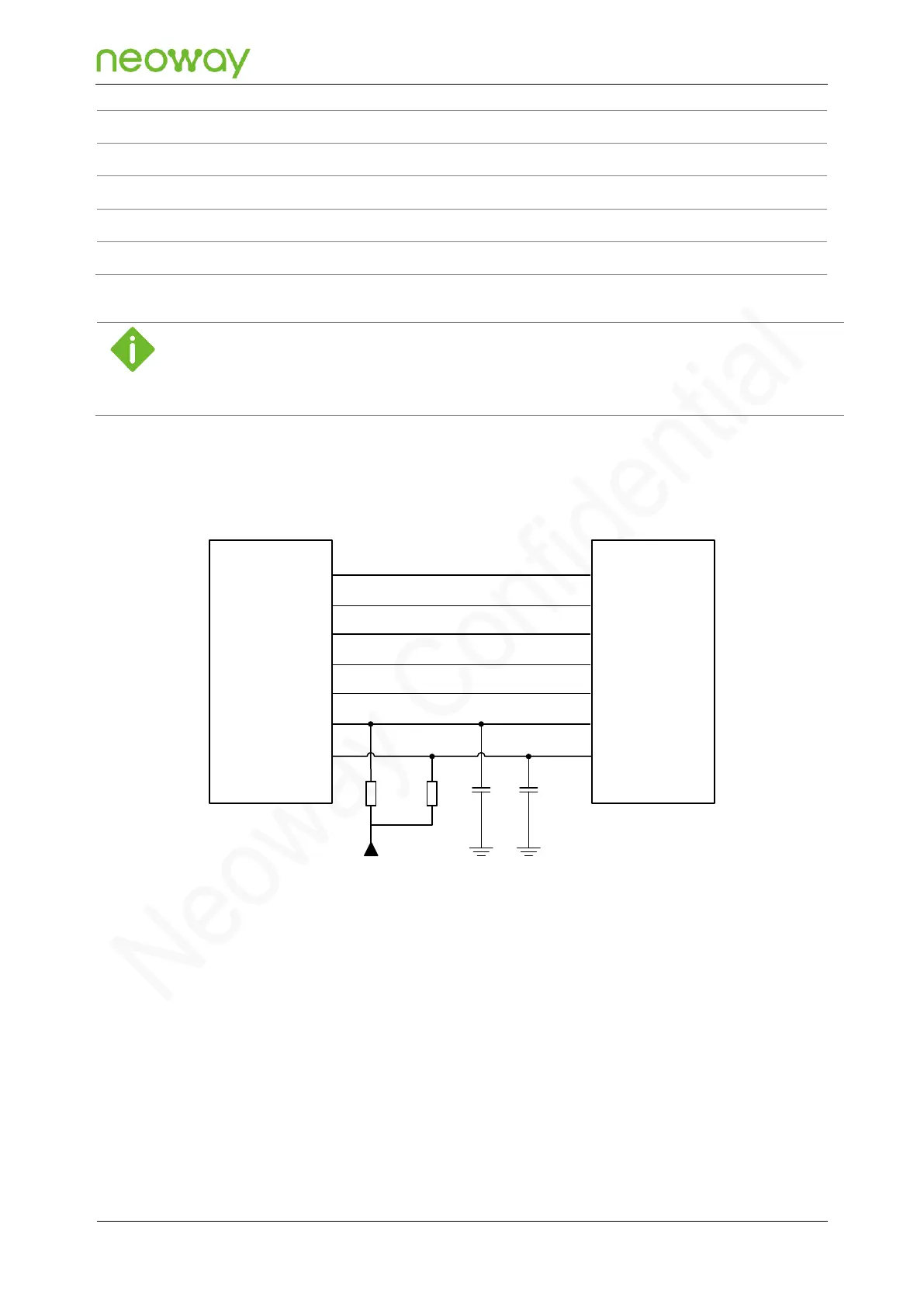
Figure 5-29 Reference design of the RMII interface
PHY
N723-EA
Module
RMII_TX_D(0~1)
RMII_RX_D(0~1)
RMII_CLK
RMII_RX_DV
RMII_TX_EN
RGMII_INT_N
RMII_RST_N
RMII_TX_D(0~1)
RMII_RX_D(0~1)
RMII_CLK
RMII_RX_DV
RMII_TX_EN
INT_N
RST_N
10KΩ
R1
10KΩ
R2
C1 C2
0.1μF 0.1μF
VDD_1P8
Design Guideline:
⚫
Pay attention to the corresponding relationship of the RMII connection. For details, read the PHY
chip manual.
⚫
Control the equal length for the TX and RX traces. For the trace length, refer to the PHY chip
manual.
⚫
Control the impedance for the TX and RX traces to 50 Ω. The clock must be wrapped by ground.
⚫
Ensure that the TX and RX trace spacing is larger than 3 times the trace width. Ensure that the
RGMII and other trace spacing is larger than 3 times the trace width.