WM620 Hardware User Guide
Copyright © Neoway Technology Co., Ltd
3 Interface Design
3.1 Power Supply and Switch Interfaces
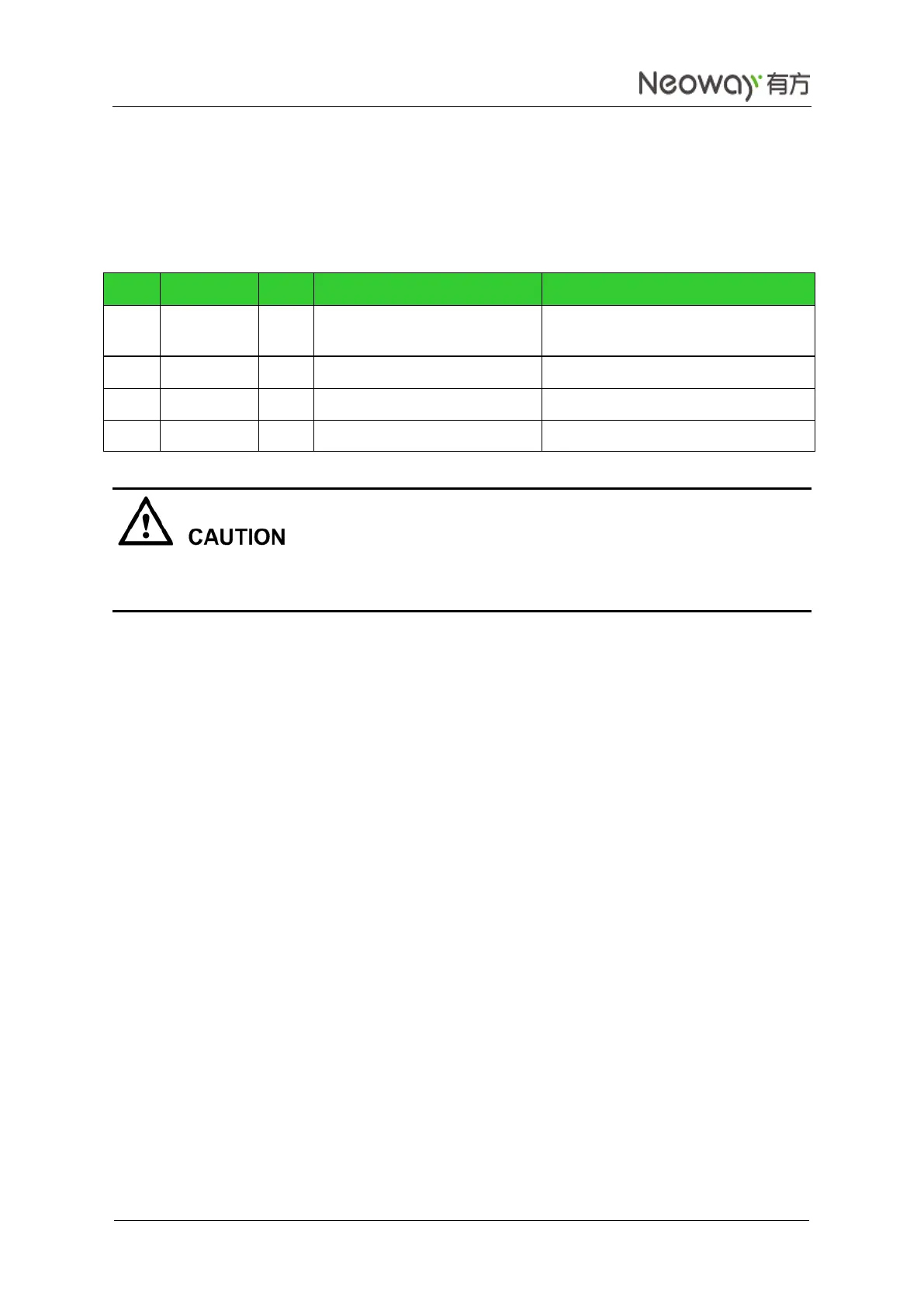
Table 3-1 Power supply and switch interface
3.3 V to 4.2 V (3.9 V is recommended)
1.8 V power supply output
2.6 V power supply output
RTC power supply input/output
Not used for any other functions
Ensure that the VBAT never exceeds 4.5 V DC. Voltage higher than 4.5 V DC may damage the WM620
module.
3.1.1 VBAT
VBAT is the main power supply of the module. Its input voltage ranges from 3.3 V to 4.2 V and the
preferable value is 3.9 V. The average current is lower than 500 mA. In addition to digital signals and
analog signals, it supplies power for RF power amplifier.
The performance of the VBAT power supply is a critical path to module's performance and stability. The
peak input current at the VBAT pin can be up to 2 A when the signal is weak and the module works at the
maximum transmitting power. The voltage will encounter a drop in such a situation. The module might
restart if the voltage drops lower than 3.3 V. Thus a large capacitor (e.g. 100 μF tantalum capacitor or 470
μF aluminum capacitor) with low ESR must be installed near the VBAT to avoid or reduce the voltage
drop caused by the RF power amplifier. Figure 3-1 shows the burst current and the voltage drops.