WM620 Hardware User Guide
Copyright © Neoway Technology Co., Ltd
3.9 RF Interface
A 50 Ω antenna is required. VSWR ranges from 1.1 to 1.5. The antenna should be well matched to
achieve best performance. It should be installed far away from high speed logic circuits, DC/DC power, or
any other strong disturbing sources.
For multiple-layer PCB, the trace between the antenna pad of module and the antenna connector, should
have a 50 Ω characteristic impedance, and be as short as possible. The trace should be surrounded by
ground copper. Dig plenty of via holes to connect this ground copper to main ground plane.
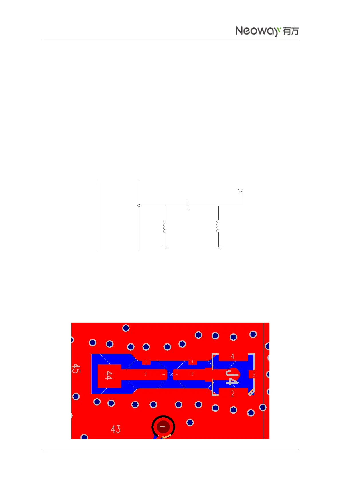
If the trace between the module and connector has to be longer, or built-in antenna is used, a π-type
matching circuit should be added, as shown in Figure 3-27. The types and values of C1, L1, and L2
should be verified by test using network analyzer instrument. If the characteristic impedance is well
matched, and VSWR requirement is met, just use a 0 Ω resistor for C1 and leave L1, L2 un-installed.
Avoid any other traces crossing the antenna trace on neighboring layer.
Figure 3-27 Reference design for antenna interface
On two-layer boards which cannot control impedance properly, the RF route should be as short and
smooth as possible and at a width of 0.8 mm to 1.0 mm; the RF is 1 mm away from the ground.
Figure 3-28 shows a two-layer board application. The RF is connected to GSC RF connector through
traces on PCB, which is connected to the antenna via cable.
Figure 3-28 RF layout reference