WM620 Hardware User Guide
Copyright © Neoway Technology Co., Ltd
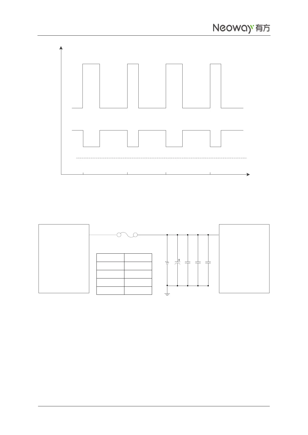
Figure 3-1 Current peaks and voltage drops
Figure 3-2 shows a recommended power supply design for the module.
Figure 3-2 Power supply design
The current test results vary with the internal impedance of the ESR capacitors and power supply. In the
above circuit, use TVS diode at D1 to enhance the performance of the module during a burst. A 100 μF
capacitor with low ESR or 470 μF aluminum capacitor is expected at C1 to reduce voltage drops during
bursts. In case of Li-ion cell battery used, a 220 μF tantalum capacitor may be applicable because the
battery has low internal impedance. In addition, add 0.1 μF, 100 pF, and 33 pF filter capacitors to filter
high frequency interference.
A controllable power supply is preferable if the module is used in harsh conditions. The WM620 module
might fail to reset in remote or unattended applications, or in an environment with great electromagnetic
interference (EMI). Users can use the EN pin on the LDO or DC/DC chipset to control the power supply
as shown in Figure 3-3 if 5 V power supply is adopted.
Keep above 3.3 V
3.3 V
0 ms
3.7 ms 7.4 ms 10.7 ms
T
2 A
Voltage
Input
Current
3.9 V
Power Supply WM620
Close to the pins
D1
C1 C2 C3 C4
VBAT
Current testing
point
I_max
C1 I_max
10uF
100uF
470uF
1000uF
2A
1.1A
0.8A
0.6A