WM620 Hardware User Guide
Copyright © Neoway Technology Co., Ltd
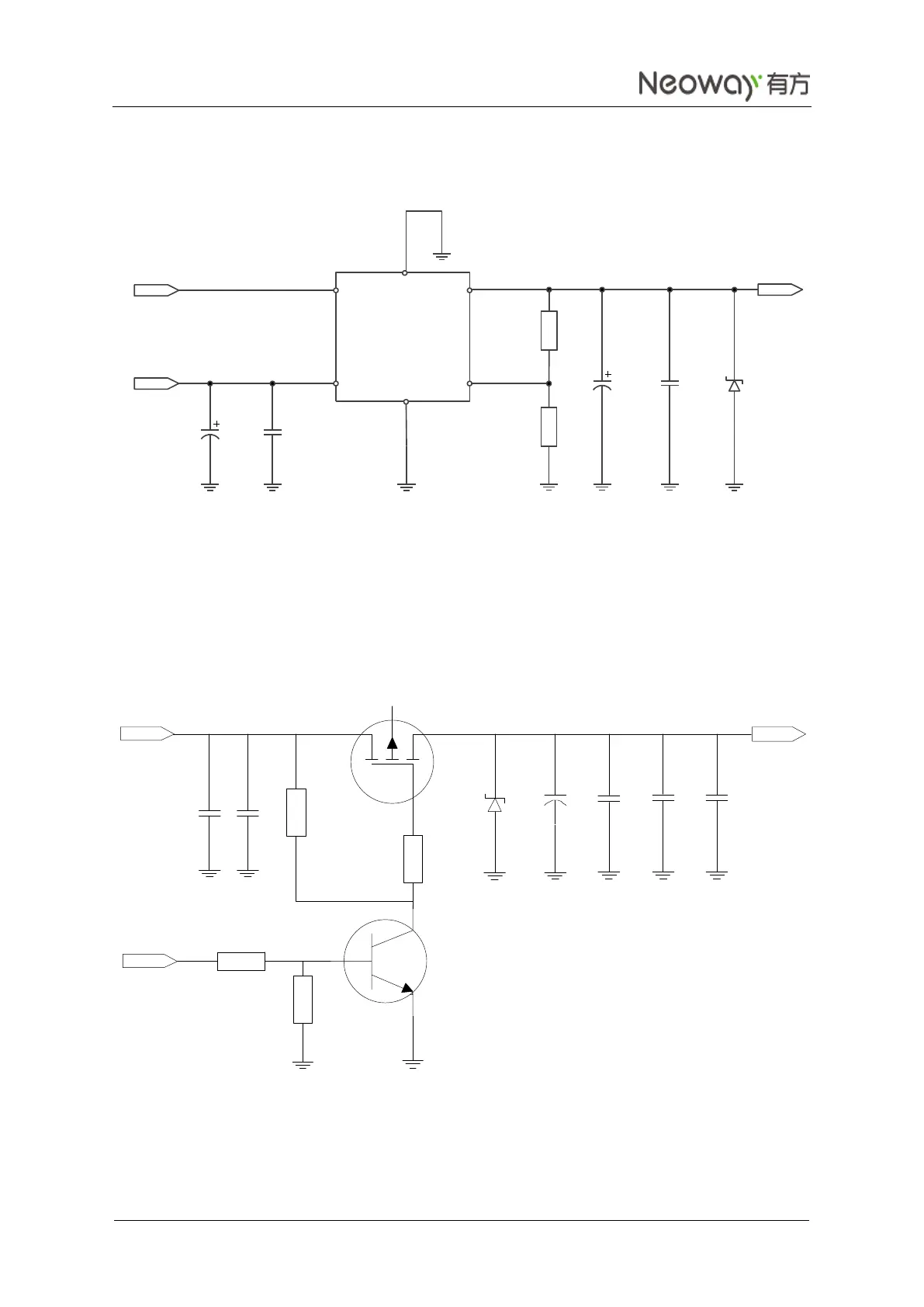
MIC29302WU in the following figure is an LDO and it can output 3 A current to ensure the performance
of the module.
Figure 3-3 Reference design of power supply controlled by MIC29302
The alternative way is to use a p-MOSFET to control the module's power supply, as shown in Figure 3-4.
This way is used if the power supply system does not consist of an EN pin. When the MCU detects the
exceptions such as no response from the module or GPRS disconnection, power-off/on can rectify the
module exceptions thoroughly. In Figure 3-4, the module is powered on when VCC_EN is set to high
level.
Figure 3-4 Reference design of power supply controlled by p-MOSFET
VDD_3.9V
VBAT
10K
100K
TVS
5V
33 pF
10 uF
470 uF
VCC_EN
2K
10K
0.1 uF
Q1
Q2
R4
C1
C2
C3
C4
C5
C6
R1
10 uF 0.1 uF
R3
INPUT
OUTPUT
D1
+
R2
In the above circuit, Q2 is added to eliminate the need for a high enough voltage level of the host GPIO.
In case that the GPIO can output a high voltage greater than VDD_3.9V - |V
GS(th)
|, where V
GS(th)
is the
Gate Threshold Voltage, Q2 is not needed.
VCCIN
VCC_EN
VBAT
100uF
TAN
0.1uF
TVS
5V
0.1uF
470uF
TAN
EN
VIN
VOUT
ADJ
MIC29302WU
10K
4.75K
C1 C2
R1
R2
C3
C4
T1