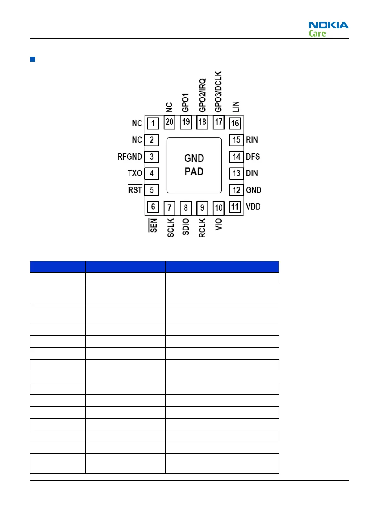
Device pin layout (Si4713-GM) and interfaces
Inteface pin descriptions
Pin Number(s) Name Description
1, 2, 20 NC No connect, left floating.
3 RFGND RF ground. Connected to ground
plane on PCB.
4 TXO FM transmitter output connection
to Tx antenna.
5 RST Device reset (active low) input.
6 SEN Serial enable input (active low).
7 SCLK Serial clock input.
8 SDIO Serial data input/output.
9 RCLK External reference oscillator input.
10 VIO I/O supply voltage.
11 VDD Supply voltage.
13 DIN Digital input data.
14 DFS Digital frame synchronisation.
15 RIN Right audio line input.
16 LIN Left audio line input.
17 GPO3/DCLK General purpose output – Digital bit
synchronous clock.
RM-505; RM-506
FMTx 2.1 Technical Description
Issue 1 COMPANY CONFIDENTIAL Page 6 –7
Copyright © 2009 Nokia. All rights reserved.