It’s possible that if GP01 and/or GPO2 are not at the correct state when the Si4713 device has power applied
then the wrong bus mode could be selected and the handset would be unable to communicate with the
device.
_SEN
The _SEN pin is used to select one of two possible 7-bit I2C bus addresses. When _SEN is low, the I2C bus
address for the Si4713 device is 0010001 (0x11). When _SEN is high, the I2C bus address for the Si4713 is
1100011 (0x63).
If the _SEN signal is not correct (i.e. not selecting the correct I2C address), then this is also another possible
reason why control of the FMTx 2.1 feature might not be possible.
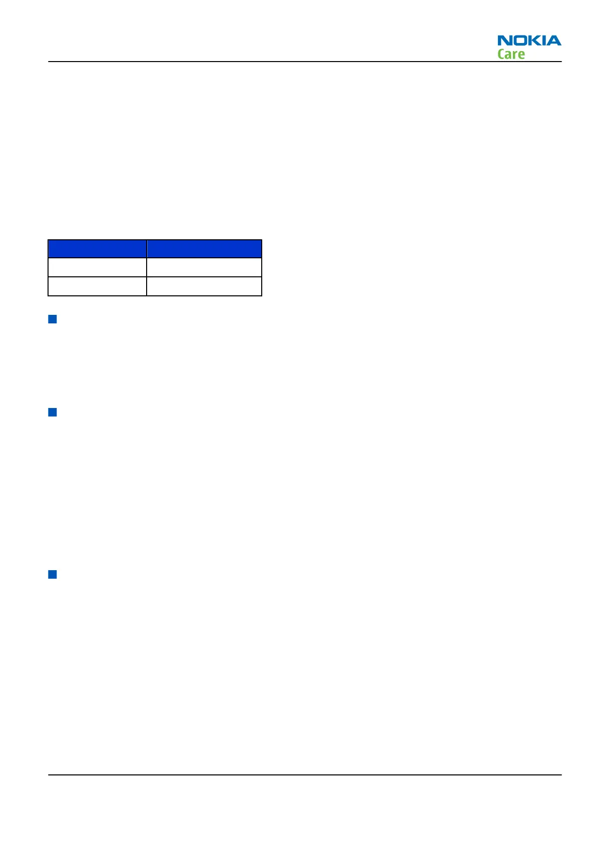
Table 11 I2C 7-bit bus address selection summary
I2C address _SEN
0010001 (0x11). High
1100011 (0x63). Low
FMTx2.1 specific RF test points
TXO
Pin 4 is the TXO pin. This is the transmitter output pin and probe access can be obtained easily. Using a high
impedance probe and a spectrum analyser it would be possible to examine the TXO pin and check that the
transmitter is outputting a signal.
Specific clock test points
RCLK
Pin 9 is the RCLK (Reference Clock) input to the device. This is typically 32.768KHz and is driven from the sleep
clock from the base band. When measuring this clock frequency, it may be seen to vary by as much as +/-
120 ~ 200ppm. The device can only typically tolerate +/- 20ppm in order to maintain transmit frequency
accuracy. To overcome this, the software driver for the device calculates what the actual sleep clock (RCLK)
frequency is and periodically programs the device with this frequency.
The device then internally adjusts its dividers in order to maintain the required output frequency. Using this
method it is possible to reduce the effective ppm of the reference clock down to +/- 14ppm over the full
operating temperature range of -15 to +50 degrees Centigrade.
General visual inspection guidelines
•
If the handset has the FMTx antenna in the back cover then check the condition of the cover, the antenna
trace and any mechanical interfaces for the antenna e.g. pogo pins.
•
Check that the Si4713 device is placed correctly on the PWB and that there are no obvious signs of damage.
•
Check the surrounding components and ensure correct placement on the PWB and that there is no visual
damage. Check that there are no missing components.
RM-505; RM-506
FMTx 2.1 Troubleshooting
Issue 1 COMPANY CONFIDENTIAL Page 7 –7
Copyright © 2009 Nokia. All rights reserved.