Power
PRELIMINARY INFORMATION
NVIDIA Jetson Orin NX DG-10931-001_v0.1 | 16
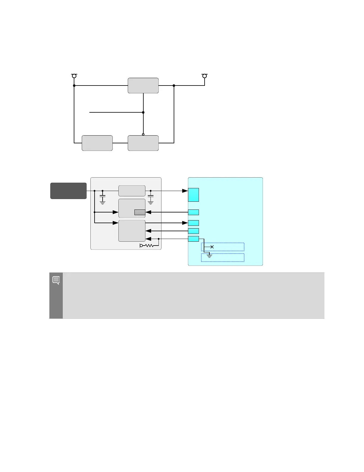
Figure 6-1. System Power and Control Block Diagram
Switch
MODULE_ ID
High Voltage
Supply
VDD_IN
(t o modul e)
Switch
5V
Supply
Module ID
= Low
Module ID =
High
EN
EN*
Figure 6-2. System Power and Control Block Diagram
Carrier Board
Main 5V – 20V
Power Source
Carri er Boa rd
Supplies
Jetson
Power Logic
POWER_EN
251
↓
260
233
SHUTDOWN_REQ*
239
SYS_RESET*
VDD_IN
EN
217
MO DUL E_ID
237
3V3_AO
Ori n NX
Legacy Module
Module
Supply
Notes:
1. MODULE_ID indicates the capability of the module. Low: Legacy module with VDD_IN = 5V
nominal.
2. Designs which implement an eFUSE or current limiting device on the input power rail of the
module should select a part that DOES NOT limit reverse current.

 Loading...


