USB and PCIe
PRELIMINARY INFORMATION
NVIDIA Jetson Orin NX DG-10931-001_v0.1 | 22
Module Pin
Recommended
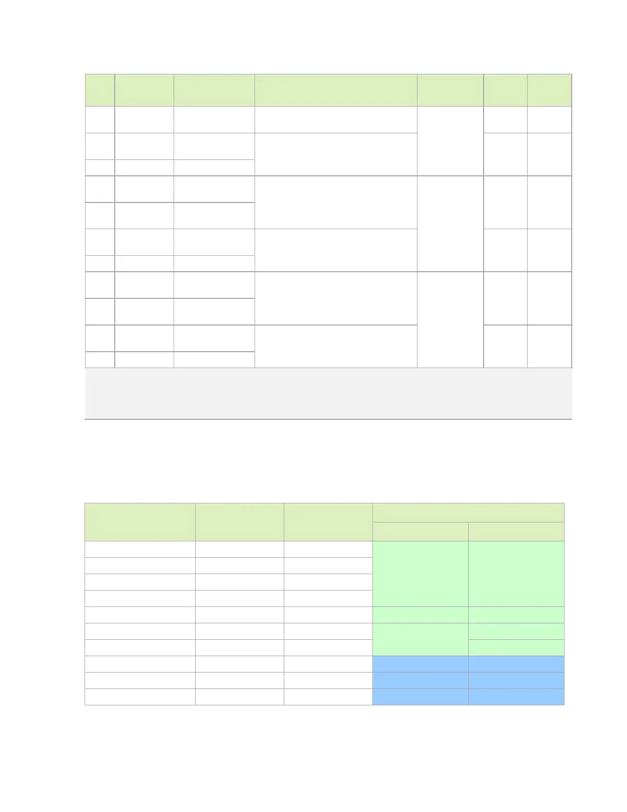
163 USBSS_RX_P
HS_UPHY0_L0_RX_
P
USB 3.2
connector,
device or hub
166 USBSS_TX_N
HS_UPHY0_L0_TX_
N
USB SS Transmit (USB 3.2 Port #0) Output
USB SS
PHY
168 USBSS_TX_P HS_UPHY0_L0_TX_P
39 DP0_TXD0_N
HS_UPHY0_L1_RX_
N
USB SS Receive (USB 3.2 Port #1)
USB 3.2
connector,
device or hub
Input
USB SS
PHY
41 DP0_TXD0_P
HS_UPHY0_L1_RX_
P
45 DP0_TXD1_N
HS_UPHY0_L1_TX_
N
USB SS Transmit (USB 3.2 Port #1) Output
USB SS
PHY
47 DP0_TXD1_P HS_UPHY0_L1_TX_P
51 DP0_TXD2_N
HS_UPHY0_L2_RX_
N
USB SS Receive (USB 3.2 Port #2)
USB 3.2
connector,
device or hub
Input
USB SS
PHY
53 DP0_TXD2_P
HS_UPHY0_L2_RX_
P
57 DP0_TXD3_N
HS_UPHY0_L2_TX_
N
USB SS Transmit (USB 3.2 Port #2) Output
USB SS
PHY
59 DP0_TXD3_P HS_UPHY0_L2_TX_P
Notes:
1. In the Direction column, Output is from Jetson Orin NX. Input is to Jetson Orin NX. Bidir is for Bidirectional signals.
2. The direction shown in this table for GPxxx_PCIEx_RST* and GP185_PCIE_WAKE* signals is true when used for those PCIe
functions. Otherwise, if used as GPIOs, the direction is bidirectional.
The following table shows the mapping options for Jetson Orin NX.
Table 7-3. USB SS and PCIe Lane Mapping
Jetson Orin NX Module
Orin NX
Orin UPHY Block
Jetson AGX Orin Configurations
PCIE0_RX0/TX0 PCIe #0 Lane 0 UPHY0, Lane 4 PCIe x4 (C4), RP/EP PCIe x4 (C4), RP/EP
PCIE0_RX1/TX1 PCIe #0 Lane 1 UPHY0, Lane 5
PCIE0_RX2/TX2 PCIe #0 Lane 2 UPHY0, Lane 6
PCIE0_RX3/TX3 PCIe #0 Lane 3 UPHY0, Lane 7
PCIE1_RX0/TX0 PCIe #1 Lane 0 UPHY0, Lane 3 PCIe x1 (C1), RP PCIe x1 (C1), RP
CSI4_D[0:2]_RX0/TX0 PCIe #2 Lane 0 UPHY2, Lane 0 PCIe x2 (C7), RP PCIe x1 (C7), RP
CSI4_D[1:3]_RX1/TX1 PCIe #2 Lane 1 UPHY2, Lane 1 PCIe x1 (C9), RP
USBSS_RX/TX USB SS #1 UPHY0, Lane 0 USB 3.2 (P0) USB 3.2 (P0)
DP0_TXD[1:0]_N/P USB SS #2 UPHY0, Lane 1 USB 3.2 (P1) USB 3.2 (P1)
DP0_TXD[3:2]_N/P USB SS #3 UPHY0, Lane 2 USB 3.2 (P2) USB 3.2 (P2)

 Loading...


