Display
PRELIMINARY INFORMATION
NVIDIA Jetson Orin NX DG-10931-001_v0.1 | 46
9.2 HDMI
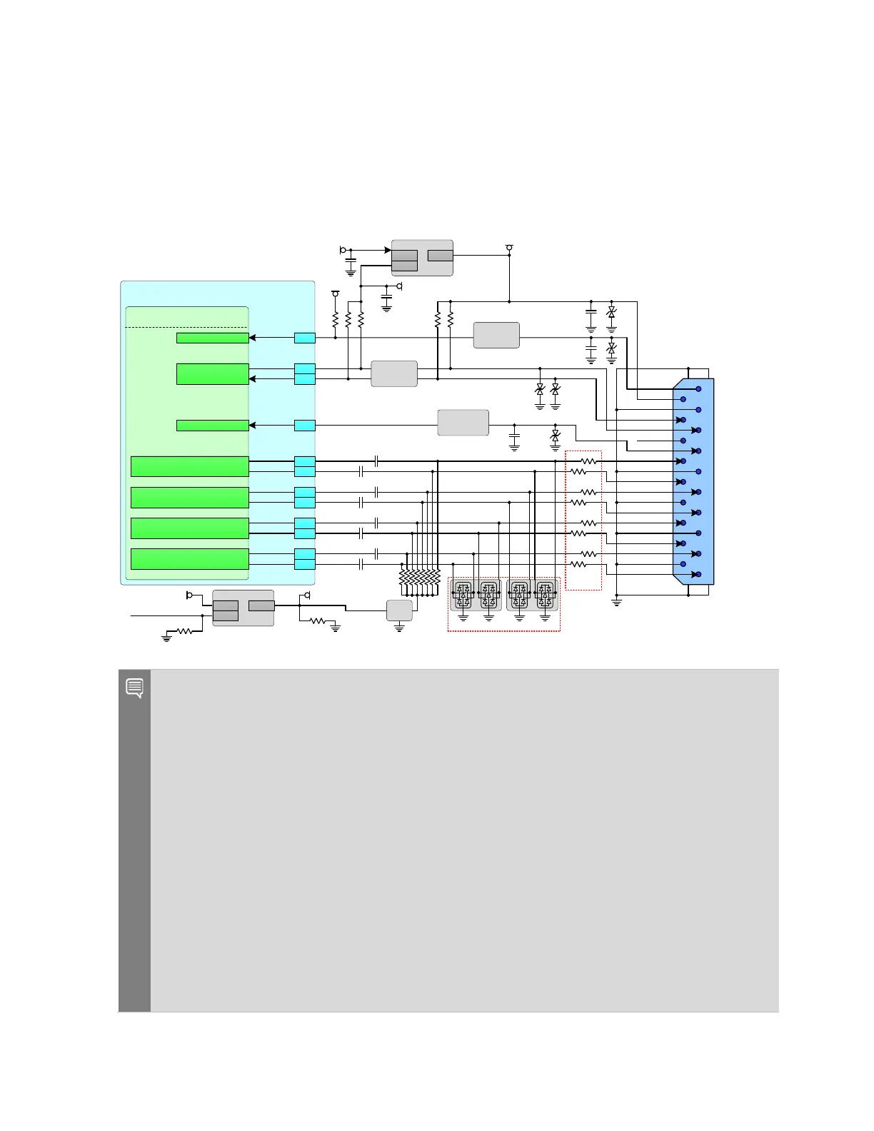
A standard DP 1.4 or HDMI v2.1 interface is supported. See Figure 9-8 for more details.
Figure 9-8. HDMI Connection Example
10 kΩ
10 kΩ
VDD_3V3_HDMI
1. 8kΩ
1. 8kΩ
VDD_5V0_HDMI_CON
10 kΩ
MOD_SLE EP*
0. 1uF
0. 1uF
0. 1uF
0. 1uF
0. 1uF
0. 1uF
0. 1uF
0. 1uF
499Ω,1%
VDD_1 V8
R
S
R
S
R
S
R
S
R
S
R
S
R
S
R
S
See
Note 4
T PD4E 02B04 DQO R
VDD_5 V_SYS
HDMI
Type A
H P_ DE T
+5V
D D C/ CE C_ GN D
SDA
SCL
RESE RVED
CEC
CK–
CK_SHIELD
CK+
D0–
D0_SH IELD
D0+
D1–
D1_SH IELD
D1+
D2–
D2_SH IELD
D2+
1
3
5
11
7
9
13
15
17
19
2
10
12
6
8
14
16
18
4
VDD_3 V3_SY S VDD_3V3_HDMI
10 kΩ
10 0kΩ
0. 1uF
Load Switch
EN
IN OUT
Lev el Sh if ter
1.8V 5V
CEC Lev el
Shifter Circuit
(se e note)
Lev el Sh if ter
3.3V 5V
Load Switch
EN
IN OUT
FET
DG
S
Jetson
SoC
– DP/HDMI
DP1_HPD
DP1_AUX_N
DP1_AUX_P
HDMI_CEC
DP1_TXD3_N
DP1_TXD3_P
DP1_TXD2_N
DP1_TXD2_P
DP1_TXD1_N
DP1_TXD1_P
DP1_TXD0_N
DP1_TXD0_P
96
100
98
65
63
71
69
77
83
81
75
HS_DISP0_HDMI_D2_DP0_P
HS_DISP0_HDMI_D2_DP0_N
HS_DISP0_HDMI_D1_DP1_P
HS_DISP0_HDMI_D1_DP1_N
HS_DISP0_HDMI_D0_DP2_P
HS_DISP0_HDMI_D0_DP2_N
HS_DISP0_HDMI_CK_DP3_P
HS_DISP0_HDMI_CK_DP3_N
SF_DPAUX01_P
SF_DPAUX01_N
GP 7 4_ HPD 0_ N
94
GP05_HDMI_CEC
Notes:
1. Level shifters required on DDC/HPD. NVIDIA Orin pads are not 5V tolerant and cannot
directly meet HDMI VIL/VIH requirements. HPD level shifter can be non-inverting or
inverting. The HPD level shifter in the reference design is inverting. The reference design
uses a BJT level shifter, and a resistor divider is needed. See the reference design if a
similar approach will be used.
2. If EMI/ESD devices are necessary, they must be tuned to minimize the impact to signal
quality, which must meet the timing and electrical requirements of the HDMI specification
for the modes to be supported. See requirements and recommendations in the related
sections of the “HDMI Interface Signal Routing Requirements” table (Table 9-5).
3. The DP1_TXx pads are native DP pads and require series AC capacitors (ACCAP) and pull-
downs (RPD) to be HDMI compliant. The 499 Ω, 1% pull-downs must be disabled when Jetson
Orin NX is off or in sleep mode to meet the HDMI VOFF requirement. The enable to the FET,
enables the pull-downs when the HDMI interface is to be used. Chokes between pull-downs
and FET are optional improvements for HDMI 2.0 operation.
4. See the RS section in Table 9-5 for details.
5.
See reference design for CEC level shifting and blocking circuit.

 Loading...


