USB and PCIe
PRELIMINARY INFORMATION
NVIDIA Jetson Orin NX DG-10931-001_v0.1 | 33
Parameter Requirement Units Notes
Gen 4.0: -9.5 dB @ 8GHz
Gen 3.0: -8.2 dB @4GHz
Max PCB via delay from the
Device/Connector
Max distance from Device ball or
Connector pin to first PCB via.
PCB within pair (intra-pair) skew
Do trace length (delay) matching before
hitting discontinuities.
Within pair (intra-pair) matching between
subsequent discontinuities
Differential pair uncoupled delay
Via
Place GND vias as symmetrically as possible to data pair vias. GND via distance
should be placed less than 1x the diff pair via pitch
Use micro via or back drilled via - no via
stub allowed.
AC Cap
20%, 0402 X5R or better. Only required
for TX pair when routed to connector.
Voiding the plane directly under the pad
~0.1mm larger than the pad size is
Serpentine (See USB 3.2 Guidelines)
Serpentine
S1 must be taken care in order to
consider Xtalk to adjacent pair. (
Min A Spacing
Min B, C Length
4x
1.5x
Trace width
Miscellaneous
Remove unwanted GND fill that is either floating or act like antenna
Connector
Void all layers of golden finger area
under the pad ~0.15mm larger than the
Keep critical PCIe traces such as PEX_TX/RX, etc. away from other signal traces or unrelated power traces and areas or power supply
components
Note:
1. This does not consider the loss of the end device or any additional connectors. These need to be accounted for and will reduce
the loss budget which will affect the max length or delay possible.
2. The max length and delay numbers are examples. These should be updated based on the actual PCB material loss and the loss
for the end device and any additional connections.
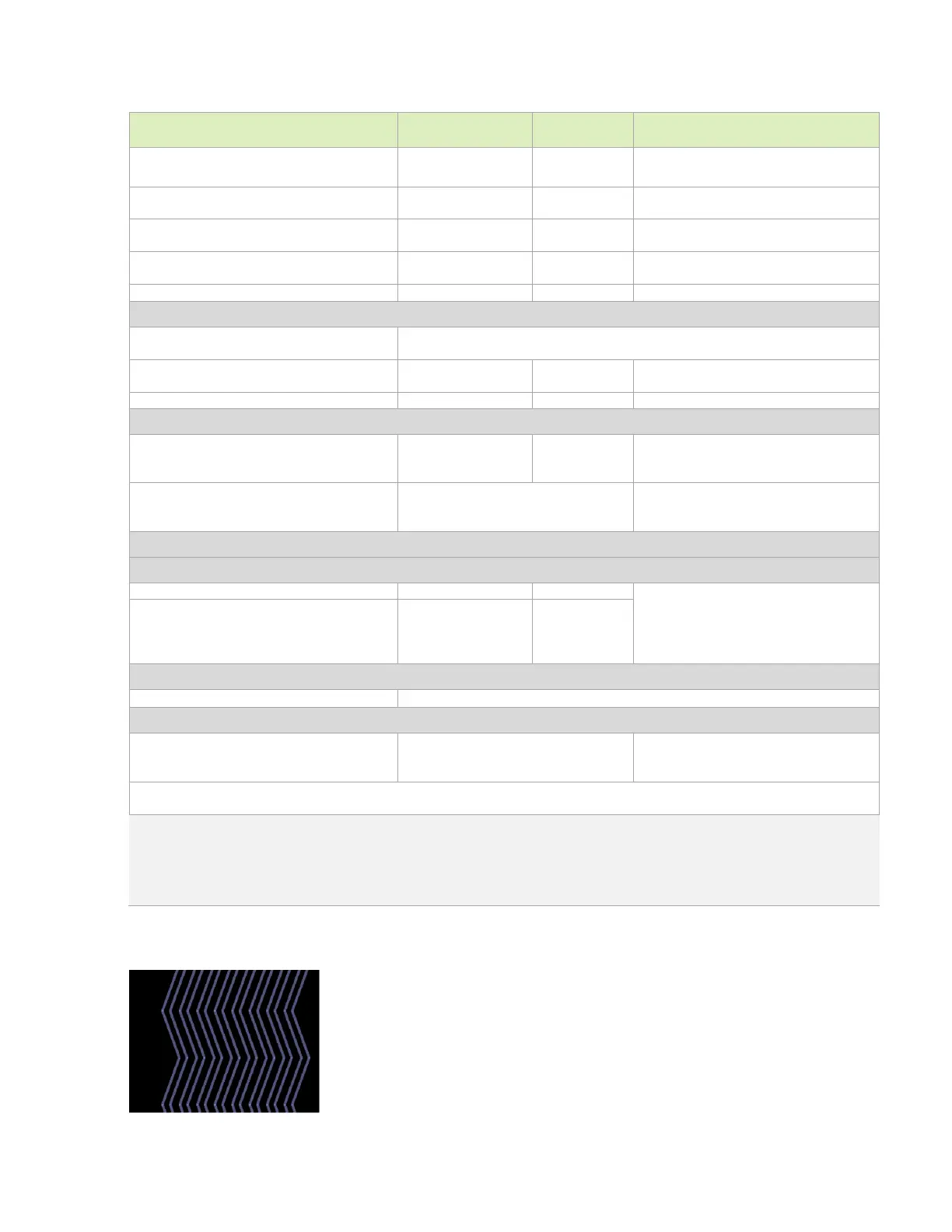
Figure 7-11. Zig-Zag Routing Example

 Loading...


