USB and PCIe
PRELIMINARY INFORMATION
NVIDIA Jetson Orin NX DG-10931-001_v0.1 | 31
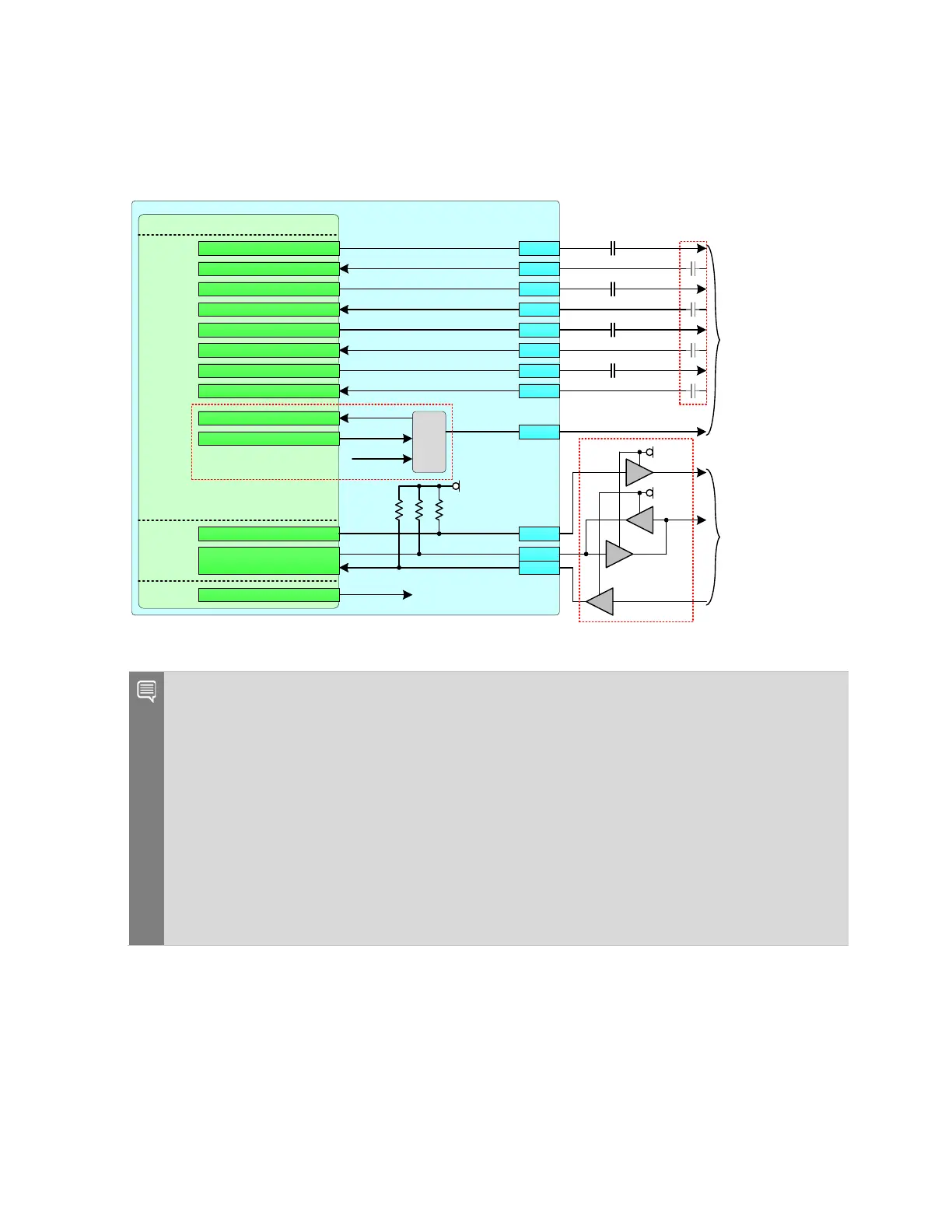
Figure 7-10 shows the x4 interface configured as Endpoint for the PCIe Endpoint connections.
Figure 7-10. PCIe Endpoint Connections Example
Jetson
SoC - PCIe
UPHY0
GP185_PCIE_WAKE_N
PEX
Ctrl
PCIe 0 Lane 3
PCIe 0 Lane 2
PCIe 0 Lane 1
PCIe 0 Lane 0
PCIE0_TX3_N/P
PCIE0_RX3_N/P
PCIE0_TX2_N/P
PCIE0_RX2_N/P
PCIE0_TX1_N/P
PCIE0_RX1_N/P
PCIE0_TX0_N/P
PCIE0_RX0_N/P
PCIE0_CLK_N/P
PCIE_WAKE*
PCIE0_CLKREQ*
PCI E 0_ RST*
3.3V
180
181
179
PCIe 0 (Ctrl # 4) –
PCIe x4 Endpoint
47kΩ
47kΩ
154/156
155/157
148/150
149/151
140/142
137/139
134/136
131/133
4.7kΩ
160/162
Mux
SE L
GP2 1
GP 21
HS_UPHY0_REFCLK2/
SF_P CIE4_CL K Mux Control
Se e N o te 2
PCIe 0 (C trl
#10) – PCIe
x4 Endpoint
OD
OD
OD
OD
3V3_E P
3V3_RP
Se e N o te 4
HS_UPHY 0
_L7_T X_ N/P
HS_UPHY 0_L7_RX_N/P
HS_UPHY 0_L6_T X_ N/P
HS_UPHY 0
_L6_RX_N/P
HS_UPHY 0
_L5_T X_ N/P
HS_UPHY 0
_L5_RX_N/P
HS_UPHY 0_L4_T X_ N/P
HS_UPHY 0
_L4_RX_N/P
HS_UPHY0_ REFCLK2_ N/P
SF_PCIE4_CLK_N/P
Se e N o te 1
GP183_PCIE4_CLKREQ _N
GP184_PCIE4_RST_N
Notes:
1. For Endpoint operation, the mux should be set to output the HS_UPHY2_REFCLK2 signals.
SoC GP21 which is used for the mux select should be set high.
2. AC capacitors required on RX lines on carrier board if connected directly to device. They
should not be on the carrier board if connected to PCIe connector, M.2 Key M, etc. In those
cases, the AC caps are on the board connected to those connectors.
3. See design guidelines for correct AC capacitor values.
4. Isolation circuitry is required on the PCIe control signals when Jetson Orin NX is configured
as Endpoint. These isolate the lines from the on-module pull-ups as well as ensure the
Endpoint and Root Port devices do not have their pads driven high before power is applied.
5. The PCIe REFCLK inputs and PCIEx_CLK clock outputs comply to the PCIe CEM specification
“REFCLK DC Specifications and AC Timing Requirements.” The clocks are HCSL compatible.
 Loading...


