Display
PRELIMINARY INFORMATION
NVIDIA Jetson Orin NX DG-10931-001_v0.1 | 45
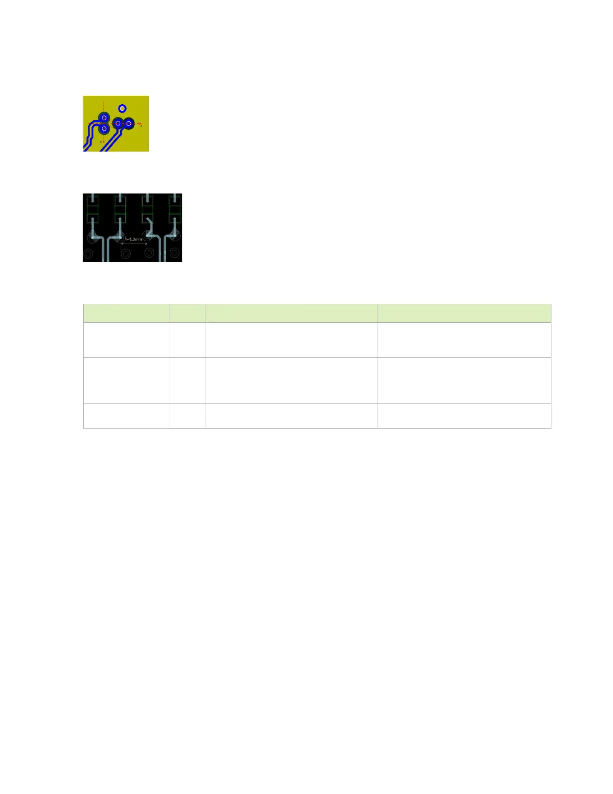
Figure 9-6. Via Topology #1
Figure 9-7. Via Topology #2
Table 9-4. eDP and DP Signal Connections
DP1_TXD[3:0]_N/P O
Series 0.1uF capacitors and ESD to
on
all.
eDP/DP Differential CLK/Data Lanes:
Connect to matching pins on display
connector.
DP1_AUX_N/P I/OD Series 0.1 uF capacitors. 100 kΩ pulldown on
DP0_AUX_P and 100kΩ pull-up to
VDD_3V3_SYS on DP0_AUX_N. ESD to
on both.
eDP/DP: Auxiliary Channels: Connect to
-/+ on display connector.
DP1_HPD I Level shifter (1.8V on module side, 3.3V on
DP/eDP connector side) and ESD to
..
eDP/DP: Hot Plug Detect: Connect to
pin on display connector through level shifter.

 Loading...


