6-87
6
Writing to Multiple Inverter Memory Registers
The writing of inverter memory registers works similar to the reading process, i.e. the address of the first reg-
ister that has to be written and the number of registers must be set in the command message.
The data registers which shall be written must be consecutive, starting from the specified address in the com-
mand message. The data order must be higher 8 bits, then lower 8 bits. The data must be in memory register
address order.
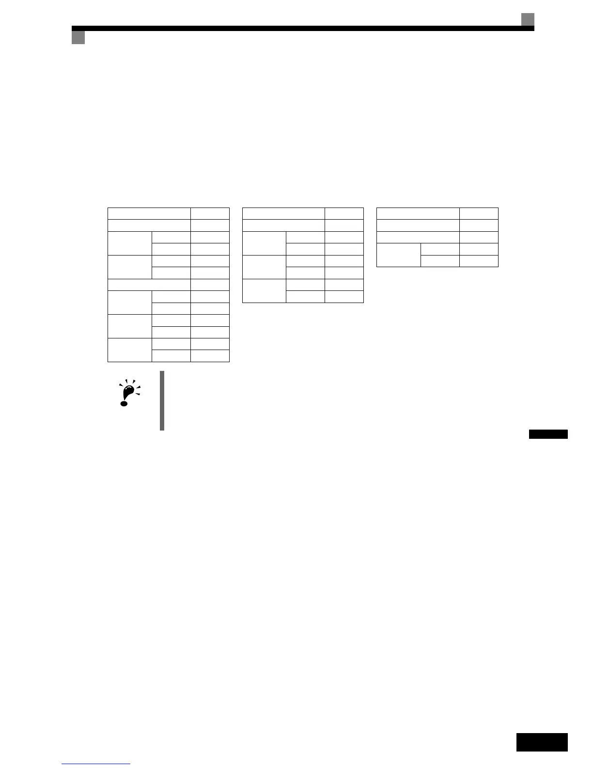
The following table shows an example of a message where a forward operation has been set with a frequency
reference of 60.0 Hz for the inverter with the slave address 01H.
Command Message
Response Message
(During Normal Operation)
Response Message
(During Error)
Slave Address 01H Slave Address 01H Slave Address 01H
Function Code 10H Function Code 10H Function Code 90H
Start Address
Higher 00H
Start Address
Higher 00H Error code 02H
Lower 01H Lower 01H
CRC-16
Higher CDH
Quantity
Higher 00H
Quantity
Higher 00H Lower C1H
Lower 02H Lower 02H
No. of data 04H
CRC-16
Higher 10H
Lead data
Higher 00H Lower 08H
Lower 01H
Next data
Higher 02H
Lower 58H * No. of data = 2 x (quantity)
CRC-16
Higher 63H
Lower 39H
IMPORTANT
For the number of data value in the command message the double value of the data quantity must be