43
[Preparation]
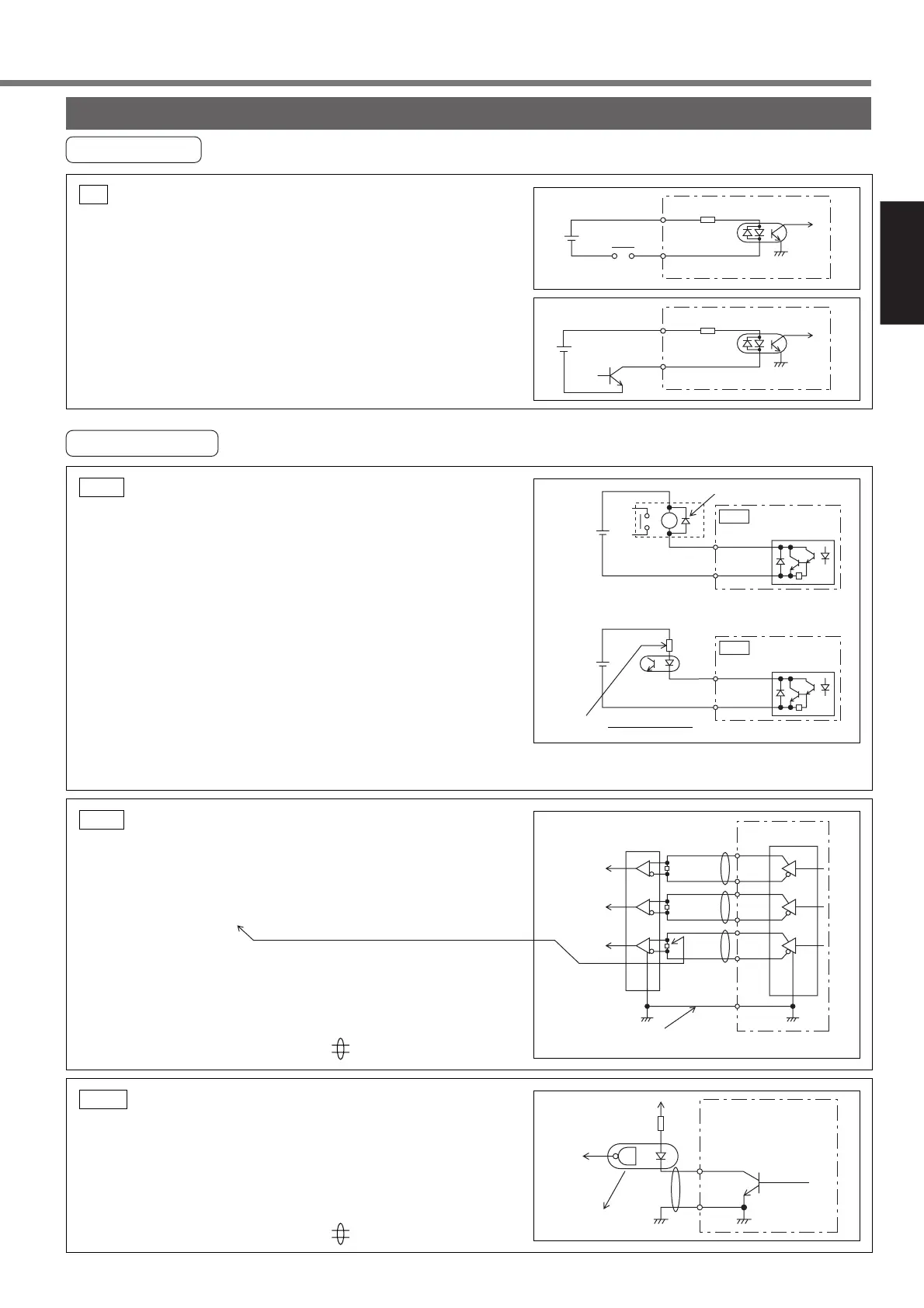
Interface Circuit
Input Circuit
Output Circuit
• Connect to contacts of switches and relays, or open collec-
tor output transistors.
• When you use contact inputs, use the switches and relays
for micro current to avoid contact failure.
• Make the lower limit voltage of the power supply (12 to 24V)
as 11.4V or more in order to secure the primary current for
photo-couplers.
Connection to sequence input signalsSI
12 to 24V
1 COM+4.7kΩ
SRV-ON etc.
Relay
1 COM+4.7kΩ
12 to 24V
SRV-ON etc.
R [kΩ] =
V
DC
[V]
–
2.5[V]
10
12 to 24V
COM–17
ALM,
COIN etc.
SO1
Max. rating 30V,50mA
12 to 24V
COM–17
ALM,
COIN etc.
SO1
Max. rating 30V,50mA
Install toward the direction.
or
• The output circuit is composed of open collector transistor
outputs in the Darlington connection, and connect to relays or
photo-couplers.
• There exists collector to emitter voltage, V
CE
(SAT) of approx.
1V at transistor-ON, due to the Darlington connection of the
output or. Note that normal TTL IC cannot be directly connec-
ted since it does not meet VIL.
• There are two types of output, one which emitter side of the
output transistor is independent and is connectable individual-
ly, and the one which is common to – side of the control pow-
er supply (COM–).
•
If a recommended primary current value of the photo-coupler is
10mA, decide the resistor value using the formula of the right Fig.
Sequence output circuitSO1
• Feeds out the divided encoder outputs (A, B and Z-phase) in
differential through each line driver.
• At the host side, receive these in line receiver. Install a termi-
nal resistor (approx. 330Ω) between line receiver inputs with-
out fail.
• These outputs are not insulated.
Line driver (Differential output) outputPO1
• Feeds out the Z-phase signal among the encoder signals in
open collector. This output is not insulated.
• Receive this output with high-speed photo couplers at the
host side, since the pulse width of the Z-phase signal is nar-
row.
Open collector outputPO2
For the recommended primary current value, refer to the data sheet of apparatus or photo-coupler to be used.
AM26LS32 or equivalent
AM26LS31 or
equivalent
A
B
Z
12
11
OA
+
OA–
OZ
+
OZ–
OB
+
OB–
13
9
26
GND
10
14
Connect signal ground of the host
and the driver without fail.
16
26
CZ
Max. rating 30V,
50mA
GND
High speed
photo-coupler
(TLP554 by Toshiba or equivalent)
represents twisted pair.
represents twisted pair.