12.2. Operation Check without Cassette Tape 55
13 Measurement And Adjustments
57
13.1. Tuner/CD Sections
57
13.2. Cassette Deck Section
57
14 Voltage Measurement and Waveform Chart
59
14.1. Waveform
62
15 Block Diagram
63
15.1. CD Servo Block
63
15.2. Main Block
65
16 Notes of Schematic Diagram
70
17 Schematic Diagram
71
17.1. CD Servo Circuit
71
17.2. Main Circuit
73
17.3. Main Control Circuit, Panel Circuit, Power-In Circuit and
Function Circuit
77
17.4. Deck Circuit, Deck Mechanism Circuit and Tape Eject
Circuit
79
17.5. Power Circuit
81
17.6. Transformer Circuit
84
17.7. CD Loading Circuit
85
18 Printed Circuit Board
86
18.1. CD Servo P.C.B.
86
18.2. Main P.C.B.
87
18.3. Main Control P.C.B. and Panel P.C.B.
89
18.4. Power In P.C.B., Function P.C.B. and Deck Mechanism
P.C.B.
90
18.5. Deck P.C.B. and Tape Eject P.C.B.
91
18.6. CD Loading P.C.B.
92
18.7. Power P.C.B.
93
18.8. Transformer P.C.B.
94
19 Wiring Connection Diagram
95
20 Illustration of IC 痴, Transistors and Diodes
97
21 Terminal Function of ICエs
98
21.1. IC702 (MN6627953HB) Servo processor/ Digital signal
processor/ Digital filter/ D/A converter
98
21.2. IC703 (BA5948FPE2) IC 4CH DRIVE
98
21.3. IC302 (C2CBJG000574) MICRO PROCESSOR
99
22 Troubleshooting Flowchart (CD Section Circuit)
101
23 Parts Location and Replacement Parts List
103
23.1. Deck Mechanism
104
23.2. CD Loading Mechanism
106
23.3. Cabinet
111
23.4. Electrical Part List
114
23.5. Packaging Materials & Accessories Parts List
122
23.6. Packaging
122
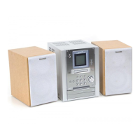
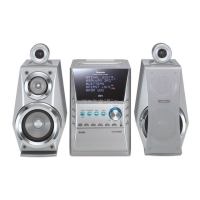
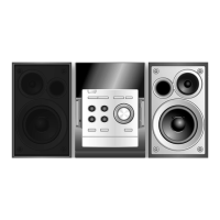
3
SA-PM31P / SA-PM31PC