Circuit Descriptions, Abbreviation List, and IC Data Sheets
EN 178 BJ2.4U/BJ2.5U LA9.
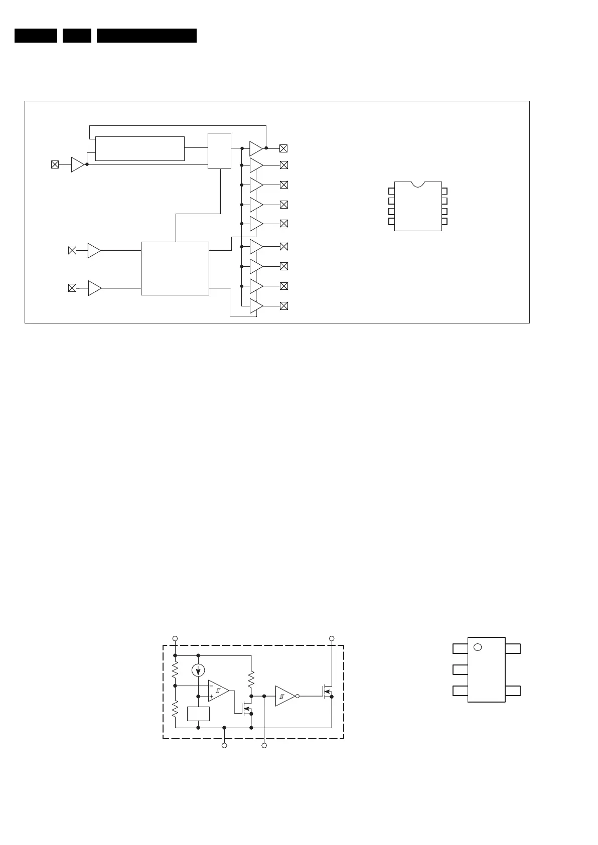
9.16.6 Diagram B4A, CY2305SC-1 (IC 7J08)
Figure 9-34 Internal block diagram and pin configuration
9.16.7 Diagram B4E, NCP303LSN (IC 7LB0 - 7LB4)
Figure 9-35 Internal block diagram and pin configuration
Block Diagram
Pin Configuration
1
2
3
4
5
8
7
6
REF
CLK2
CLK1
GND
V
DD
CLKOUT
CLK4
CLK3
SOIC
CY2305SC-1
Top View
PLL
MUX
Select Input
REF
S2
S1
CLKA1
CLKA2
CLKA3
CLKA4
CLKB1
CLKB2
CLKB3
CLKB4
Decoding
CLKOUT
E_14620_146.eps
241004
Block Diagram
Pin Configuration
F_15400_133.eps
230905
NCP303LSNxxT1
Open Drain Output Configuration
V
ref
2 Input
3 Gnd
5C
D
R
D
1 Reset Output
1
3
N.C.
Reset
Output
2
Input
Ground
4
C
D
5
xxxYW
(Top View)
xxx = 302 or 303
Y = Year
W = Work Week
 Loading...