Circuit Descriptions, Abbreviation List, and IC Data Sheets
EN 204 JL2.1E AA9.
Stand-by Supply
The Stand-by Supply is based upon the "Fly Back Converter"
principle. A description of this principle can be found in the
FM2x Service Manuals.
Specifications
• Class D audio amplifier on same panel.
• Low profile.
• Full range (90 - 270 V
AC
) and for all screen sizes (however
NOT exchangeable due to component diversity).
Outputs
• +5V2.
• +5V_SW (switched "off" in stand-by).
• V_TUN (Tuner voltage, switched "off" in stand-by).
Inputs
• 130-400 V
DC
from the Mains Filter panel (1306).
• STANDBY_INFO from SSB (1M03).
• Over-voltage / safety protection from the Main Supply
(1307 -> 6150/51/53 -> 7150 -> 7505/09 -> 7560).
– Protection against over-voltage of the mains.
– Protection against short-circuit of mains elco’s with
doubler.
Interfacing between SSB and Main Supply
• +24V (or +12V) from MF supply (1304) to Display
(backlight) (1312, 1313, or 1314, 1315 or 1316, 1317).
• +12V from MF supply (1304) to SSB (1M46) and Ambient
Light circuit (1M10).
9.2.3 Start-up Sequence
Connect the Mains Voltage
1. A voltage of 130-400 V
DC
(depends on region) will be
available at the Stand-by Supply panel.
2. The +5V2 becomes available for the SSB.
Close the Functional Switch
1. +5V2_RELAY_IO will be present (= supply for relay and
uP). A POR is generated.
2. If STANDBY bit is "low", the +5V_SW will be present for the
SSB.
3. The relay is closed.
4. The Main Supply will start up.
5. The +24V (+12V for Sharp displays) and the Audio Supply
becomes available.
6. +12V ready from MF panel -> +8V6 on Stand-by Supply
panel is ready to SSB
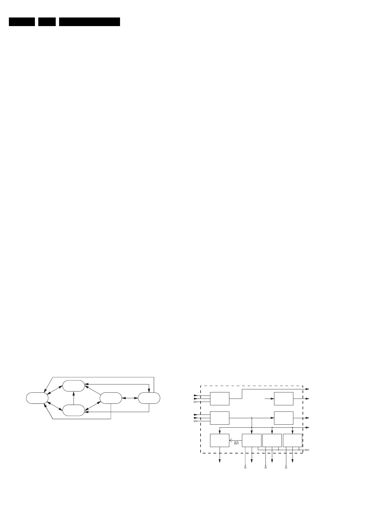
9.2.4 Power States
There are four different power states.
Figure 9-7 Power state diagram
• OUT: The set is OUT when the mains cord is disconnected.
When the mains cord is connected, the set goes to OFF or
to STANDBY state, depending on the last status in the
NVM. From all states, the set can be set to the OUT state
by disconnecting the mains cord or by a mains interruption.
• OFF: In the OFF state, the OTC is powered but is in low
power STANDBY state. No LEDs are "on", RC6 is ignored,
no EPG or P50 is possible, Proximity is set to "off", time
extraction is not started (if it was done before this state, the
clock stays running). This state can only be changed by the
tact switch; the set goes via SEMI-STANDBY to ON. From
all states, we can go to the OFF state by the tact switch.
• STANDBY: The set is in STANDBY if the STANDBY bit is
set. This state can change with the RC6 "on" command, for
EPG loading, P50 recording, for time extraction, or for
ambient light. The next state is SEMI-STANDBY and to ON
if the STANDBY bit is not set.
• SEMI-STANDBY: State between STANDBY or OFF and
ON state. All supply voltages are present, but the screen is
blanked.
• ON: set is ON.
Notes:
• In SEMI-STANDBY coming from STANDBY, the blue LED
is "on",
• In SEMI-STANDBY coming from ON, the red LED is "on".
9.2.5 POR Detection
Since the ON/OFF switch is always closed (not present any
more), there is no POR by starting up. The POR line is
connected to +5V2 and is always "high". Only when the mains
cord is reconnected, the Stand-by supply starts up, and the
POR line follows the start up of the 5V2
9.3 DC/DC Converters (on SSB)
9.3.1 Introduction
The LCD Supply and Stand-by Supply are the main power
supplies for this chassis. They deliver the following supply
voltages to the SSB (connector 1M46):
• +12VS.
• +8V6.
• +5V2.
•+5V.
•+VTUN.
As the VIPER and many other ICs on the SSB require low
supply voltages at high current (up to 3 A for the main
voltages), on board DC/DC converters are implemented.
The circuit on the SSP provides the 3.3 V, 2.5 V, and 1.2 V.
A DC/DC converter has the following advantages:
• The DC/DC converter is directly on the SSB near the
circuits that needs to be powered.
• Some circuits on the SSB need high current by low voltage,
so there is no risk to have power dips or voltage loss in
connections between the PSU and the SSB panel.
9.3.2 Block Diagram
See also diagram B1.
Figure 9-8 DC/DC converter block diagram
E_14620_020.eps
290404
OUT ONSemi Standby
OFF
Standby
8V6
SWITCH
+5V
+8V6
+8V6-SW
+2V5D
+2V5
+12VSW
SUPPLY-FAULT
ON-MODE
+2V5D
LINEAR
STABILISER
+5V2_STBY
12V
SWITCH
+12VSW
+1V2
ENABLE-1V2
VSW
VTUN
GENERATOR
12V/1V2
DC/DC CONV.
12V/3V3
DC/DC CONV.
+12VS
+5V
POD-MODE
+2V5
LINEAR
STABILISER
+3V3VTUN
ENABLE-3V3
F_15400_004.eps
280905
(Reserved)
(Reserved)
(Reserved)
12V/2V5
DC/DC CONV.
+2V5
ENABLE-2V5