Circuit Descriptions, Abbreviation List, and IC Data Sheets
EN 205JL2.1E AA 9.
9.3.3 Start-up Sequence
1. If the input voltage of the DC/DC converters is around 12 V
(measured on the decoupling capacitors 2U17/2U25/
2U45) and the ENABLE signals are "low" (active), then the
output voltages should have their normal values.
2. First, the Stand-by Processor activates the +1V2 supply
(via ENABLE-1V2).
3. Then, after this voltage becomes present and is detected
OK (about 100 ms), the other two voltages (+2V5 and
+3V3) will be activated (via ENABLE-3V3).
4. The current consumption of controller IC 7U00 is around 20
mA (that means around 200 mV drop voltage across
resistor 3U22).
9.3.4 1.2V, 2.5V, and 3.3V DC/DC Converters
Introduction
The circuits use a so-called "synchronous buck converter".
Some characteristics:
• Switching frequency: approx. 250 kHz.
• Efficiency: approx. 90%.
• Built-in output over-voltage and over-current protections
• Soft start.
• Software controlled “on/off” (via ENABLE line).
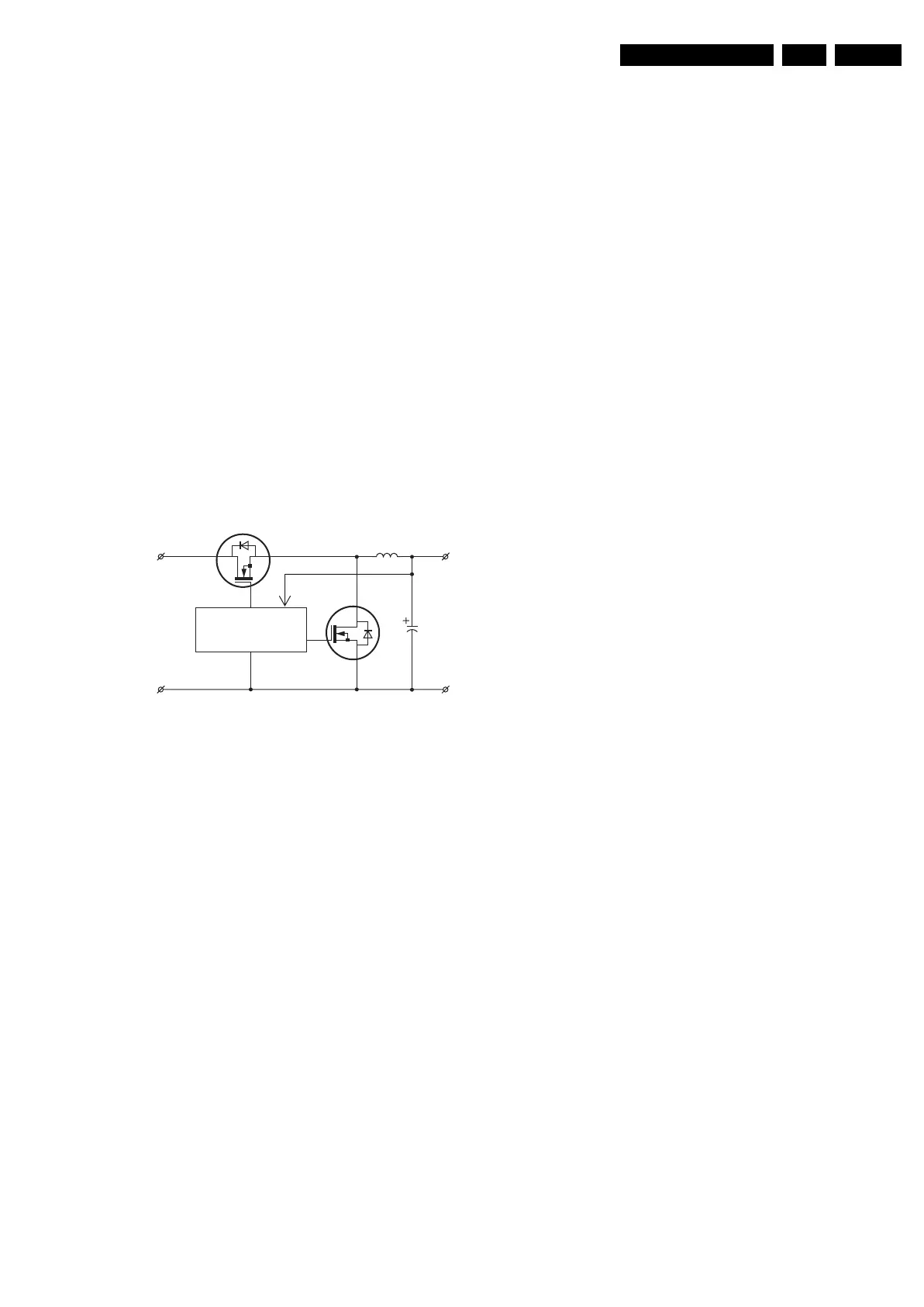
Block Diagram
Figure 9-9 Block diagram synchronous buck converter.
The advantage of a "synchronous buck converter" over a
"classical buck converter" is its better efficiency (about 90%).
The difference between the two is that in a synchronous buck
converter the "low -side" diode is replaced by a MOSFET TS2.
This, because the voltage drop across a MOSFET is smaller
than the forward voltage drop of a diode.
This second MOSFET TS2 conducts current during the "off"
times of the first MOSFET TS1. The upper MOSFET TS1
conducts, to transfer energy from the input to the inductor L
1
and load R
L
, while the lower MOSFET TS2 conducts to
circulate the inductor current (free wheel). The synchronous
PWM control block regulates the output voltage by modulating
the conduction intervals of the upper and lower MOSFETs.
12 V to 1.2 V DC/DC converter (7U06)
This circuit is activated when the ENABLE-1V2 signal is “low”.
The network 3U26+2U91+3UA7 delays the switch “off” of the
converter in case of a power drop on +5V2.
The controller IC contains the error amplifier, a reference
voltage of 0.9 V 2% (pin 1), an oscillator (250 kHz, set by
resistor 3U31), driver stages for the output MOS-FETs 7U03-1
and 7U03-2 (pins 11: HGATE and 14: LGATE), and a window
comparator for the output voltage (it has as output PGOOD pin,
connected to SUPPLY-FAULT signal).
The output voltage is set by resistors 3U04, 3U28, and 3U30
and filtered by 2U39 and 5U06 for medium frequency
(switching frequency) and 2U59, 5U09, 5U12, 5U13, and 5U14
for high frequency (tenths of MHz).
A boost voltage (peaks of 22 V) is provided by components
2U28 and 6U03 to pin 12 for properly driving the transistor
7U03-1.
The output voltage is ramped-up in about 5 ms (set by value of
capacitor 2U19).
Additional AC-feedback for stability of converter (components
2U43, 2U54, 2U57,3U39 and 3U42).
The switching speed of 7U03-A is reduced for noise reason by
means of components 2U86, 3U49, and 3U96.
The output over-voltage protection (crowbar action) and over-
current protection (6…8A) is set by resistor 3U14.
12 V to 2.5 V DC/DC converter (7U05)
Is almost similar to the 12 V to 1.2 V DC/DC converter, but is
providing two output voltages: +2V5 and +2V5D (separated by
Schottky diodes).
It is started after the 12 V to 1.2 V DC/DC converter, by making
the ENABLE-2V5 line “low”.
12 V to 3.3V DC/DC converter (7U04)
Is similar to the 12 V to 1.2 V DC/DC converter, but is providing
3.3 V and is started together with the 12 V to 2.5 V DC/DC
converter by making its enable signal ENABLE-3V3 “low”.
Service Tips
• When a power MOS-FET is found defective, replace the
other power MOS-FET and fuse 1U01 as well.
• For a normal operation of the converter, it is important to
check the switching frequency, the value of the boost
voltage, and the amplitude of the gate voltage of transistor
7U04 (it should be close to the boost voltage).
9.3.5 +2V5D Linear Stabiliser (7U19)
• Provides the +2V5D voltage for the DDR memory chips of
the VIPER, and is derived from the +5V2-STBY voltage
coming from the Main Power Supply.
• The output current is limited to a few tenths of mA.
• Output over-voltage protection is done by zener diode
6U17.
9.3.6 Internal Protection (7U20)
• This circuit around 7U20 provides a SUPPLY-FAULT
signal (active "low"), when the output voltage of any DC/DC
converter is out of its limits (± 10% of the normal value). In
such cases, the Stand-by Processor will immediately stop
the supplies by sending a "high" control signal towards the
external and internal supplies: ENABLE-xVx, ON-MODE,
and STAND-BY.
Note: The SUPPLY-FAULT control signal is "low" when
any DC/DC converter is disabled by its control signal
(ENABLE-xVx) and +12VSW is present, therefore it is
ignored during start-up!
• The internal protection works also together with the over-
voltage detection transistors 7U08-2, 7U09-2, 7U10-2, and
the PGOOD pin of the controller ICs (7U04, 7U05, and
7U06).
9.3.7 +12V Under-voltage Detection (7UB1)
This circuit around 7UB1 detects when the incoming +12V
drops below 9 V and then switches “off” the 2.5 V and 3.3V DC/
DC converters. In this way, the power “off” sequence of the
VIPER (+3V3, +2V5, and +2V5D must drop before the +1V2
drops) is guaranteed.
9.3.8 Indicator LEDs (6U22, 6U23, 6U24)
They provide a visual indication on the availability of the +1V2,
+2V5, and +3V3 voltages.
F_15400_005.eps
090505
D
S
G
D
Vin
S
G
PWM GENERATOR
& MOSFET DRIVER
GND
Vout
GND
C1
TS2
FB
TS1
L1