Circuit Descriptions, Abbreviation List, and IC Data Sheets
EN 216 JL2.1E AA9.
9.10 PNX2015: LVDS Transmitter (if used)
Low Voltage Differential Signalling (LVDS) is a low-power, low-
noise differential technology for high speed data transmission
over two PWB traces, or a balanced cable. LVDS allows single-
channel data transmission at hundreds, or even up to a
thousand Mbps. Low swing and current-mode driver outputs
create low noise and provide very low power consumption
across frequency ranges.
The LVDS transmitter IP provides a connection interface to
FPDs.
Differences between standard and LVDS signalling:
• Standard single ended signal (TTL):
– Requires 28 signal lines and more than 14 grounds.
– Single ended signals up to 3 V.
– Wide flat ribbon cable.
– EMI/EMC problems.
– Feasible up to VGA/NTSC resolution (limited to 250
Mb/s).
• LVDS:
– Five low voltage (350 mV) differential pairs: one clock
pair and four data pairs.
– Five grounds.
– EMI/EMC friendly.
– WXGA and HD-1280x720p (up to 1 Gb/s).
LVDS offers superior performance compared to the standard
single ended signal (TTL).
It is even "protocol independent" so it requires no software.
Figure 9-28 LVDS technology
The digital video output from the VIPER is connected to the
display via the LVDS interface. This transmitter converts 28 bits
of LVCMOS/LVTTL data into four LVDS (Low Voltage
Differential Signalling) data streams. A phase-locked transmit
clock is transmitted in parallel with the data streams over a fifth
LVDS link. With every cycle of the transmit clock, 28 bits of
input data are sampled and transmitted. At a transmit clock
frequency of 85 MHz, 24 bits of RGB data and 3 bits of LCD
timing and control data (FPLINE, FPFRAME, DRDY) are
transmitted at a rate of 595 Mbps per LVDS data channel.
Using a 85 MHz clock, the data throughput is 297.5 Mbytes/
sec.
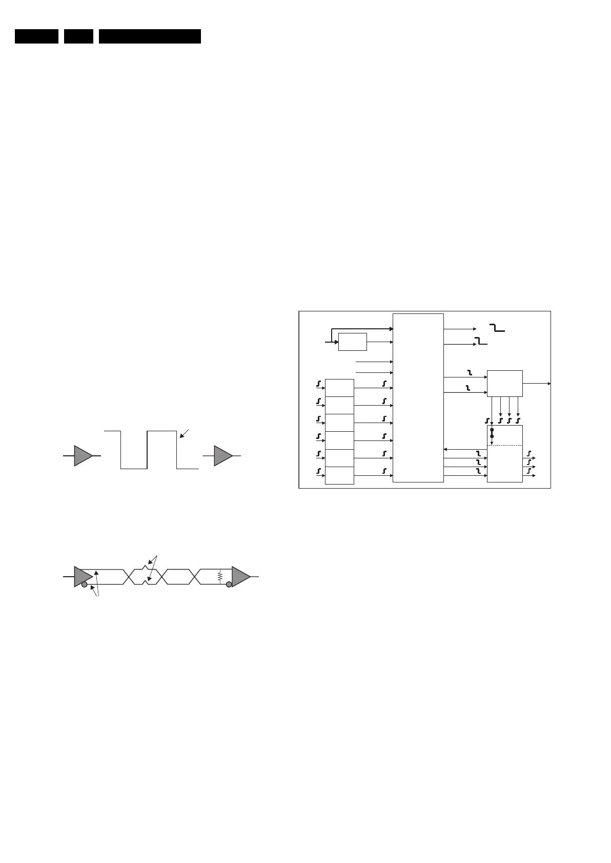
9.11 PNX2015: Stand-by Processor
9.11.1 Introduction
The Stand-by Processor’s sub system is isolated from the other
sub systems within thePNX2015. It has its own power supply
(1.2V and 3.3V), together with separate clocking (16MHz) and
reset. This allows for it to be active while all other sub systems
are either inactive, via clock being disabled, or powered down.
The main tasks of the Stand-by Controller are:
• RC5/RC6 remote control handling.
• P50.
• Keyboard handling (side control, “on/off” switch).
• Detection and protection of the power supplies.
• Status detection on EXTernals.
• SAM/SDM entering.
• Provide boot-scripts to the VIPER.
• Start-up behaviour of the set; sequentially enabling the
power supplies via the ENABLE lines.
9.11.2 TV Start-up Behaviour and Fault Detection
Figure 9-29 Start-up behaviour
1. The Stand-by Controller is powered by the +5V2 voltage
(3V3_STBY voltage is derived from the +5V2), which
becomes available when the set is connected to the Mains
/ AC Power.
2. By default, all I/O lines of the controller are “high”, this state
is also the state that will not trigger protections or cause
supplies to rise, since enabling a supply requires that an IO
line is pulled "low". Also all protections are active "low".
3. The 16 MHz crystal starts running.
4. Reset IC 7M03 will generate a RESET_STBY pulse.
5. All I/O lines will be set in default state, as “told” by the
software.
– RESET_SYSTEM will be "low" (this will hold the
VIPER in reset).
– LAMP_ON will be "low".
6. The system waits for an RC or functional switch command:
when this command is "low" the set will start-up.
F_15710_174.eps
230905
10 10
Standard Single Ended Single Signal & Larger
Voltage swing
Low Voltage Differential Signalling
Two Signals & Smaller Voltage Swing
Noise
- Lower Voltage Swing (only 350 mV vs. 3 V)
- Standard open Ended: 250Mbps
- LVDS: >1 Gbps
- Allows faster Clocking
- Differential Signals (Two Signals) ...Low Noise!
- Receiver reads a 1 or 0 based on the delta of the two signals.
- Noise Impacts both lines and cancels out each others.
10 1 0
F_15710_182.eps
260905
Detect 1V2
Detect 2V5
Detect 3V3
Detect 8V6
Detect 12V
Detect 5V
Reset µC
1V2
2V5
3V3
Supply-fault
1V2
2V5
3V3
5V
8V6
12Vsw
1V2
2V5
3V3
Enable-1V2
Enable-2V5
Enable-3V3
Detect-2V5
Detect-3V3
Detect-5V
Detect-8V6
Detect-12V
Detect-1V2
LSP power
supply
standby
+12V
+8V6
+5V
Vtun
Lamp On
+12V/+24V
Reset-system
On boards
DC/DC
Converters
P2.0
P2.1
P2.2
P2.5
P2.3
P2.4
P1.3
PNX2015
Vdd
reset-µc P3.4
P0.2
P0.3
P0.4
P0.5
P4.0
Reset-main NVM
P4.6
P0.0
P2.7
Prot Audio Supply
P3.2
Power Ok platform 3V3
3V3 Stby
Detect 1V2
Detect 2V5
Detect 3V3
Detect 8V6
Detect 12V
Detect 5V
Reset µC
1V2
2V5
3V3
Supply-fault
1V2
2V5
3V3
5V
8V6
12Vsw
1V2
2V5
3V3
Enable-1V2
Enable-2V5
Enable-3V3
Detect-2V5
Detect-3V3
Detect-5V
Detect-8V6
Detect-12V
Detect-1V2
Power
supply
standby
+12V
+8V6
+5V
Vtun
Lamp On
+12V/+24V
Reset-system
On board
DC/DC
Converters
P2.0
P2.1
P2.2
P2.5
P2.3
P2.4
P1.3
PNX2015
Vdd
reset
-
µc P3.4
P0.2
P0.3
P0.4
P0.5
P4.0
Reset-main NVM
P4.6
P0.0
P2.7
Prot Audio Supply
P3.2
Power Ok platform 3V3
3V3 Stby
Standby to on