Pin Connect Block 129 May 03, 2004
Philips Semiconductors Preliminary User Manual
LPC2119/2129/2194/2292/2294ARM-based Microcontroller
Pin Function Select Register 2 (PINSEL2 - 0xE002C014)
The PINSEL2 register controls the functions of the pins as per the settings listed in Table 63. The direction control bit in the
IO1DIR register is effective only when the GPIO function is selected for a pin. For other functions direction is controlled
automatically.
Warning: use read-modify-write operation when accessing PINSEL2 register. Accidental write of 0 to bit 2 and/or bit 3 results in
loss of debug and/or trace functionality! Changing of either bit 4 or bit 5 from 1 to 0 may cause an incorrect code execution!
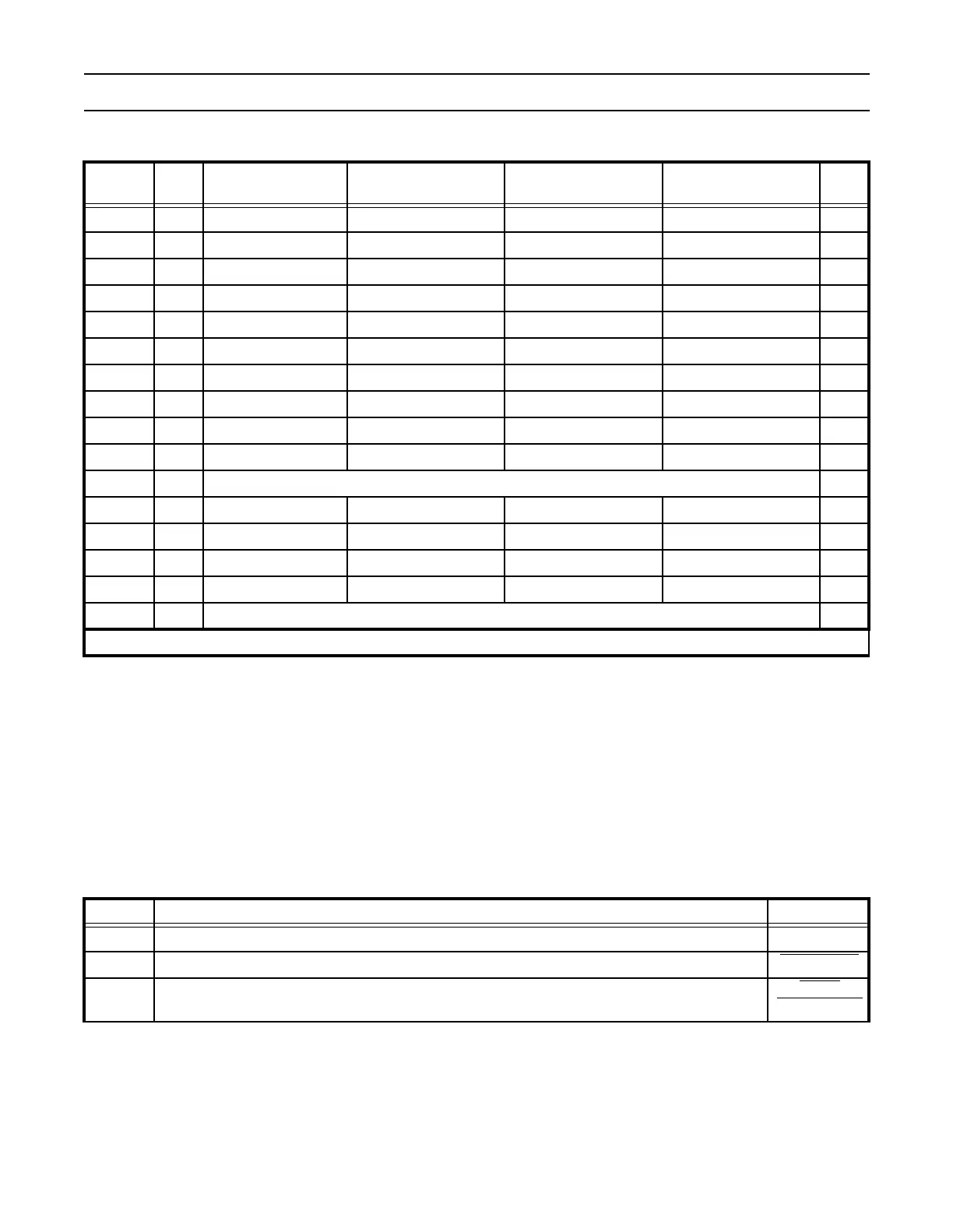
Table 62: Pin Function Select Register 1 for LPC2194/2294 (PINSEL1 - 0xE002C004)
PINSEL1
Pin
Name
Function when 00 Function when 01 Function when 10 Function when 11
Reset
Value
1:0 P0.16 GPIO Port 0.16 EINT0 Match 0.2 (TIMER0) Capture 0.2 (TIMER0) 00
3:2 P0.17 GPIO Port 0.17 Capture 1.2 (TIMER1) SCK (SPI1) Match 1.2 (TIMER1) 00
5:4 P0.18 GPIO Port 0.18 Capture 1.3 (TIMER1) MISO (SPI1) Match 1.3 (TIMER1) 00
7:6 P0.19 GPIO Port 0.19 Match 1.2 (TIMER1) MOSI (SPI1) Match 1.3 (TIMER1) 00
9:8 P0.20 GPIO Port 0.20 Match 1.3 (TIMER1) SSEL (SPI1) EINT3 00
11:10 P0.21 GPIO Port 0.21 PWM5 RD3
1
(CAN Controller 3) Capture 1.3 (TIMER1) 00
13:12 P0.22 GPIO Port 0.22 TD3
1
(CAN Controller 3) Capture 0.0 (TIMER0) Match 0.0 (TIMER0) 00
15:14 P0.23 GPIO Port 0.23 RD2 (CAN Controller 2) Reserved Reserved 00
17:16 P0.24 GPIO Port 0.24 TD2 (CAN Controller 2) Reserved Reserved 00
19:18 P0.25 GPIO Port 0.25 RD1 (CAN Controller 1) Reserved Reserved 00
21:20 P0.26 Reserved 00
23:22 P0.27 GPIO Port 0.27 AIN0 (A/D Converter) Capture 0.1 (TIMER0) Match 0.1 (TIMER0) 01
25:24 P0.28 GPIO Port 0.28 AIN1 (A/D Converter) Capture 0.2 (TIMER0) Match 0.2 (TIMER0) 01
27:26 P0.29 GPIO Port 0.29 AIN2 (A/D Converter) Capture 0.3 (TIMER0) Match 0.3 (TIMER0) 01
29:28 P0.30 GPIO Port 0.30 AIN3 (A/D Converter) EINT3 Capture 0.0 (TIMER0) 01
31:30 P0.31 Reserved 00
1
CAN Controller 3 is available in LPC2294 only. Fields in the table related to CAN3 have Reserved value for all other parts.
Table 63: Pin Function Select Register 2 for LPC2119/2129/2194 (PINSEL2 - 0xE002C014)
PINSEL2 Description Reset Value
1:0 Reserved. 00
2 When 0, pins P1.36:26 are used as GPIO pins. When 1, P1.31:26 are used as a Debug port. P1.26/RTCK
3 When 0, pins P1.25:16 are used as GPIO pins. When 1, P1.25:16 are used as a Trace port.
P1.20/
TRACESYNC