External Memory Controller (EMC) 59 May 03, 2004
Philips Semiconductors Preliminary User Manual
LPC2119/2129/2194/2292/2294ARM-based Microcontroller
EXTERNAL MEMORY INTERFACE
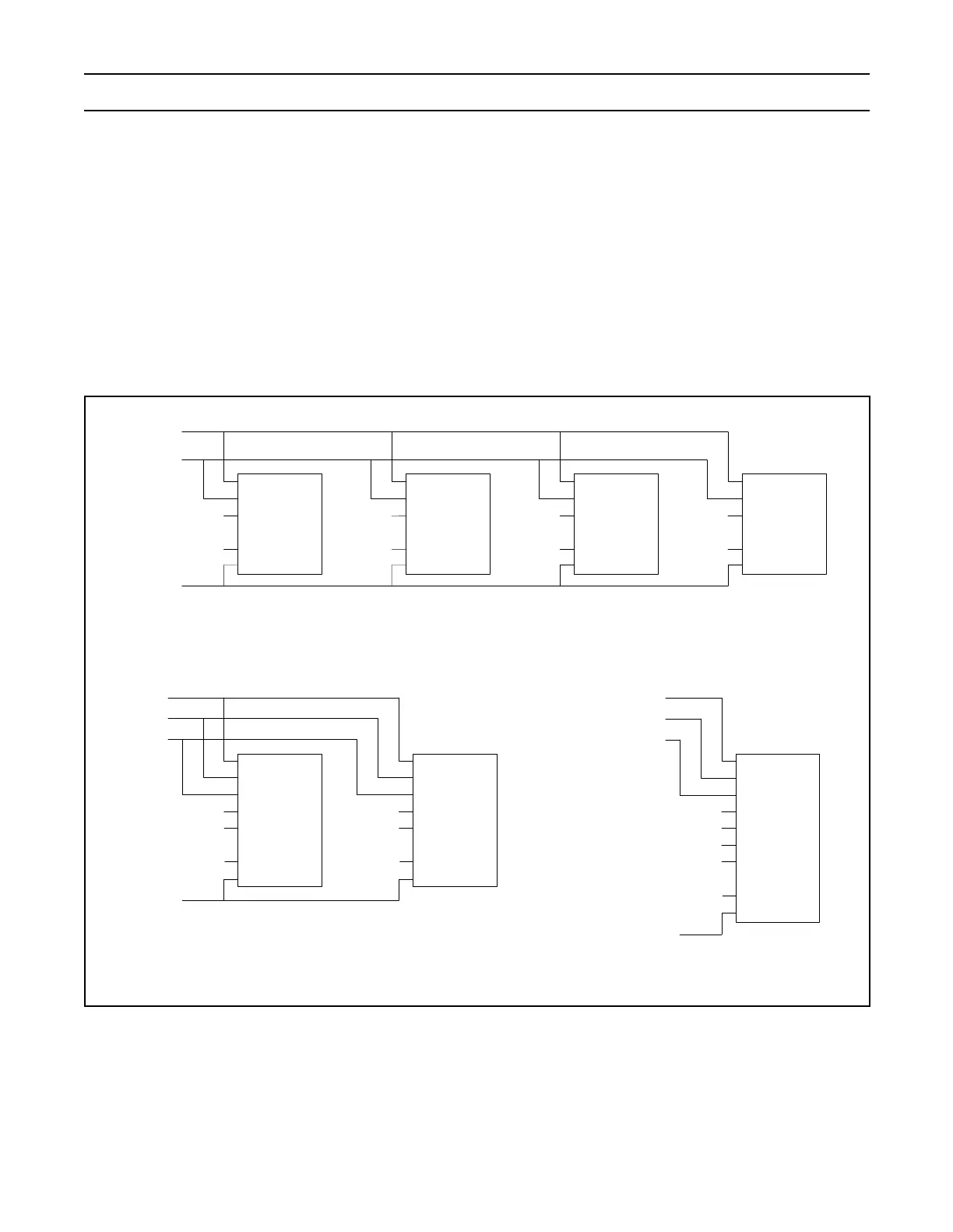
External memory interface depends on the bank width (32, 16 or 8 bit selected via MW bits in corresponding BCFG register).
Furthermore, choice of the memory chip(s) will require an adequate setup of RBLE bit in BCFG register, too. RBLE = 0 in case
of 8-bit based external memories, while memory chips capable of accepting 16 or 32 bit wide data will work with RBLE = 1.
If a memory bank is configured to be 32 bits wide, address lines A0 and A1 can be used as non-address lines. Memory bank
configured to 16 bits wide will not require A0, while 8 bit wide memory bank will require address lines down to A0. Configuring
A1 and/or A0 line(s) to provide address or non-address function is acomplished using bits 23 and 24 in Pin Function Select
Register 2 (PINSEL2 register).
Symbol "a_b" in following figures refers to the highest order address line in the data bus. Symbol "a_m" refers to the highest order
address line of the memory chip used in the external memory interface
Figure 7: 32 Bit Bank External Memory Interfaces
A[a_b:2]
BLS[1]
D[15:8]
CE
OE
WE
IO[7:0]
A[a_m:0]
BLS[0]
D[7:0]
CE
OE
WE
IO[7:0]
A[a_m:0]
OE
CS
BLS[3]
D[31:24]
CE
OE
WE
IO[7:0]
A[a_m:0]
BLS[2]
D[23:16]
CE
OE
WE
IO[7:0]
A[a_m:0]
a) 32 bit wide memory bank interfaced to 8 bit memory chips
b) 32 bit wide memory bank interfaced to 16 bit memory chips
OE
CS
WE
CE
OE
WE
B3
B2
B1
B0
IO[31:0]
A[a_m:0]
D[31:0]
BLS[2]
A[a_b:0]
BLS[3]
BLS[0]
BLS[1]
c) 32 bit wide memory bank interfaced
to 32 bit memory chip
OE
CS
WE
CE
OE
WE
UB
LB
IO[15:0]
A[a_m:0]
D[31:16]
BLS[2]
CE
OE
WE
UB
LB
IO[15:0]
A[a_m:0]
D[15:0]
BLS[0]
A[a_b:2]
BLS[3]
BLS[1]