System Control Block 76 May 03, 2004
Philips Semiconductors Preliminary User Manual
LPC2119/2129/2194/2292/2294ARM-based Microcontroller
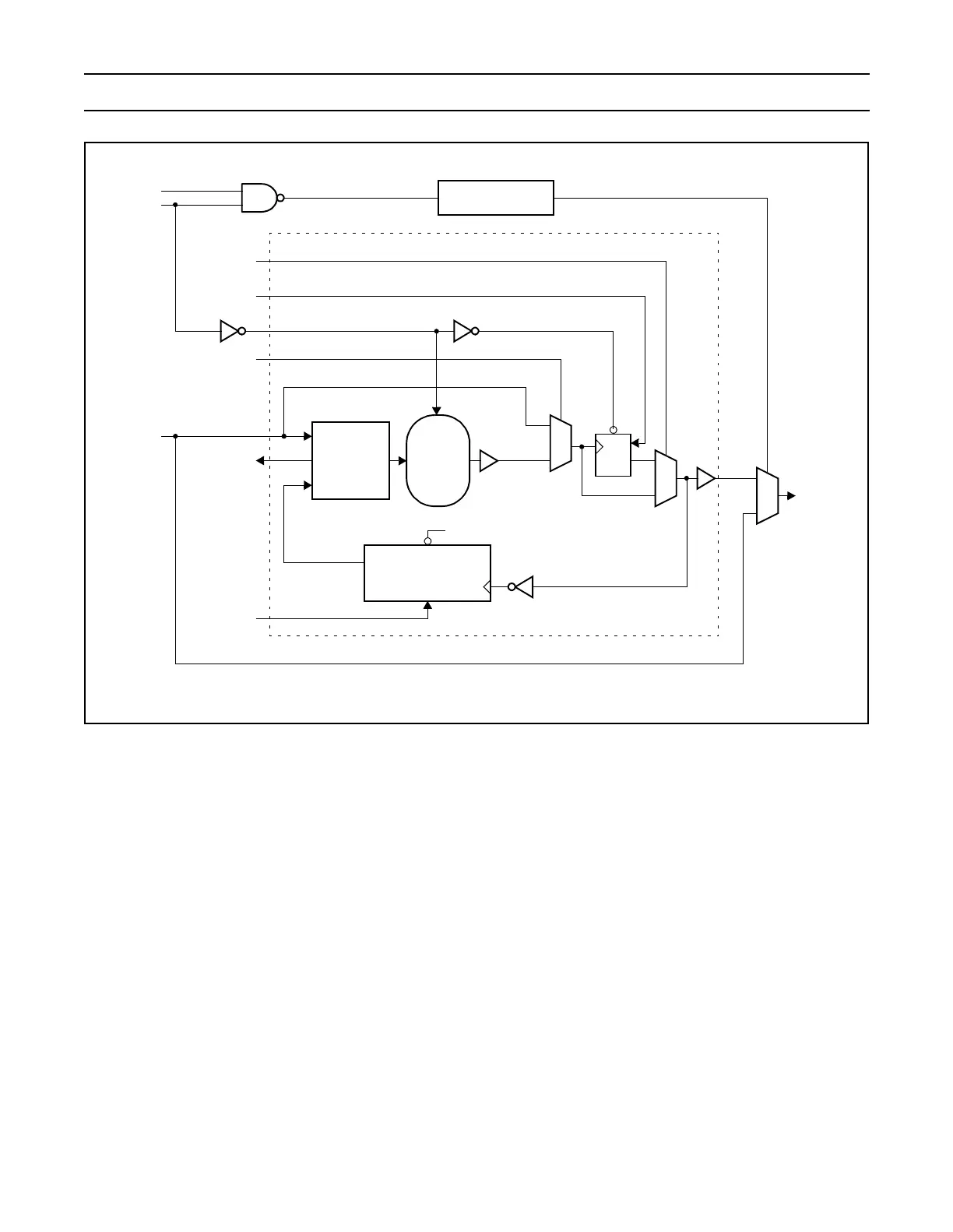
Figure 15: PLL Block Diagram
PLL Control Register (PLLCON - 0xE01FC080)
The PLLCON register contains the bits that enable and connect the PLL. Enabling the PLL allows it to attempt to lock to the
current settings of the multiplier and divider values. Connecting the PLL causes the processor and all chip functions to run from
the PLL output clock. Changes to the PLLCON register do not take effect until a correct PLL feed sequence has been given (see
PLL Feed Register (PLLFEED - 0xE01FC08C) description).
CCO
Phase-
Frequency
Detector
F
OSC
PLOCK
Bypass
msel<4:0>
Div-by-M
pd
MSEL[4:0]
PSEL[1:0]
fout
cd
1
0
1
cd
/2P
PLLC
Direct
PLLE
cclk
F
CCO
pd
0
pd
0
1
0
0
Clock
Synchronization