System Control Block 67 May 03, 2004
Philips Semiconductors Preliminary User Manual
LPC2119/2129/2194/2292/2294ARM-based Microcontroller
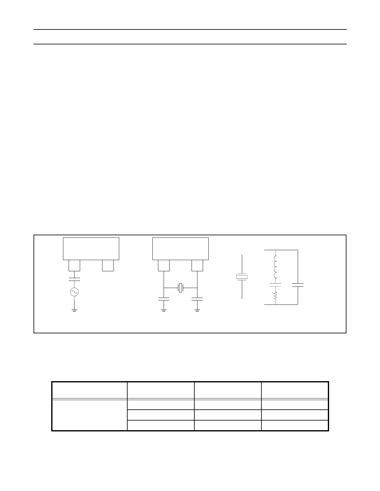
CRYSTAL OSCILLATOR
While an input signal of 50-50 duty cycle within a frequency range from 1 MHz to 50 MHz can be used by LPC2119/2129/2194/
2292/2294 if supplied to its input XTAL1 pin, this microcontroller’s onboard oscillator circuit supports external crystals in the range
of 1 MHz to 30 MHz only. If on-chip PLL system or boot-loader is used, input clock frequency is limited to exclusive range of 10
MHz to 25 MHz.
The oscillator output frequency is called F
osc
and the ARM processor clock frequency is referred to as cclk for purposes of rate
equations, etc. elsewhere in this document. F
osc
and cclk are the same value unless the PLL is running and connected. Refer to
the PLL description in this chapter for details and frequency limitations.
Onboard oscillator in LPC2119/2129/2194/2292/2294 can operate in one of two modes: slave mode and oscillation mode.
In slave mode the input clock signal should be coupled by means of a capacitor of 100 pF (Cc in Figure 12, drawing a), with an
amplitude of at least 200 mVrms. X2 pin in this configuration can be left not connected. If slave mode is selected, F
osc
signal of
50-50 duty cycle can range from 1 MHz to 50 MHz.
External components and models used in oscillation mode are shown in Figure 12, drawings b and c, and in Table 13. Since the
feedback resistance is integrated on chip, only a crystal and the capacitances C
X1
and C
X2
need to be connected externally in
case of fundamental mode oscillation (the fundamental frequency is represented by L, C
L
and R
S
). Capacitance Cp in Figure 12,
drawing c, represents the parallel package capacitance and should not be larger than 7 pF. Parameters F
C
, C
L
, R
S
and C
P
are
supplied by the crystal manufacturer.
Choosing an oscillation mode as an on-board oscillator mode of operation limits F
osc
clock selection to 1 MHz to 30 MHz.
Figure 12: Oscillator modes and models: a) slave mode of operation, b) oscillation mode of operation,
c) external crystal model used for C
X1/X2
evaluation
Table 13: Recommended values for C
X1/X2
in oscillation mode (crystal and external components parameters)
Fundamental Oscillation
Frequency F
C
Crystal Load
Capacitance C
L
Max. Crystal Series
Resistence R
S
External Load
Capacitors C
X1
, C
X2
1 - 5 MHz
10 pF n.a. n.a.
20 pF n.a. n.a.
30 pF < 300 : 58 pF, 58 pF
C
L
R
S
C
P
L
<=>
X1 X2
C
X1
C
X2
Xtal
X1 X2
C
C
Clock
a) b) c)
LPC2119/29/94
LPC2292/2294
LPC2119/29/94
LPC2292/2294