EmbeddedICE Logic 287 May 03, 2004
Philips Semiconductors Preliminary User Manual
LPC2119/2129/2194/2292/2294ARM-based Microcontroller
PIN DESCRIPTION
RESET STATE OF MULTIPLEXED PINS
On the LPC2119/2129/2194/2292/2294, the pins above are multiplexed with P1.31-26. To have them come up as a Debug port,
connect a weak bias resistor (4.7 k:) between VSS and the P1.26/RTCK pin. To have them come up as GPIO pins, do not
connect a bias resistor, and ensure that any external driver connected to P1.26/RTCK is either driving high, or is in high-
impedance state, during Reset.
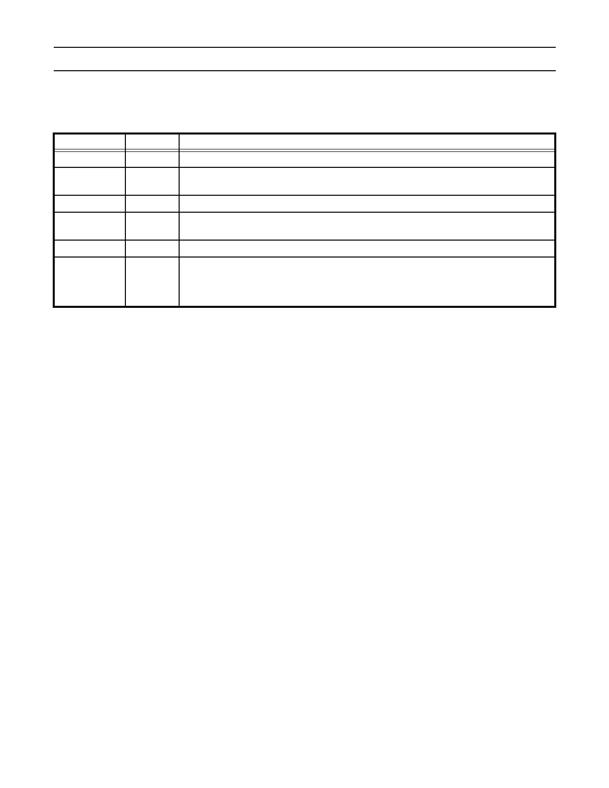
Table 223: EmbeddedICE Pin Description
Pin Name Type Description
TMS Input Test Mode Select. The TMS pin selects the next state in the TAP state machine.
TCK Input
Test Clock. This allows shifting of the data in, on the TMS and TDI pins. It is a positive edge-
triggered clock with the TMS and TCK signals that define the internal state of the device.
TDI Input Test Data In. This is the serial data input for the shift register.
TDO Output
Test Data Output. This is the serial data output from the shift register. Data is shifted out of the
device on the negative edge of the TCK signal
nTRST Input Test Reset. The nTRST pin can be used to reset the test logic within the EmbeddedICE logic.
RTCK Output
Returned Test Clock. Extra signal added to the JTAG port. Required for designs based on
ARM7TDMI-S processor core. Multi-ICE (Development system from ARM) uses this signal to
maintain synchronization with targets having slow or widely varying clock frequency. For details
refer to "Multi-ICE System Design considerations Application Note 72 (ARM DAI 0072A)".