146
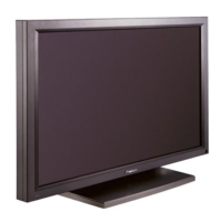
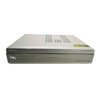
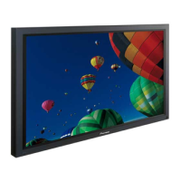
PDP-433CMX
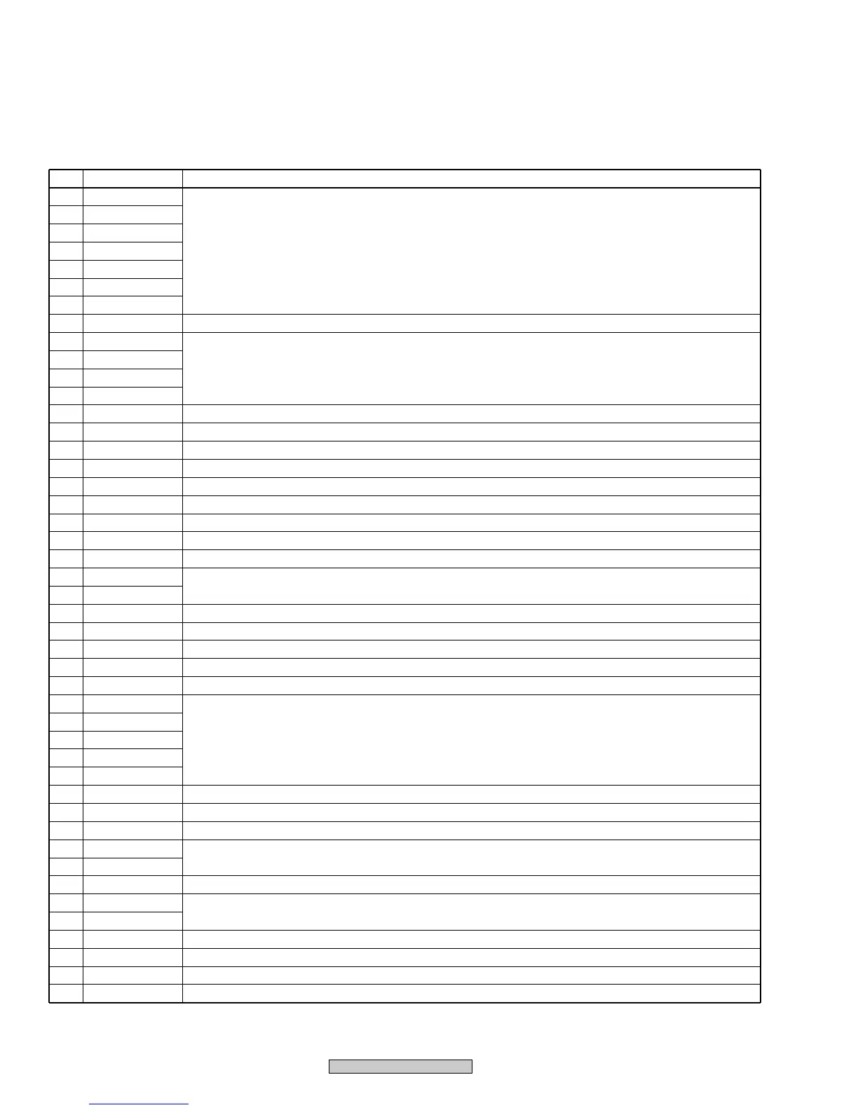
No. Pin Name Function
46 UD5
47 UD6
48 UD7
49 UD8
50 UD9
51 UD10
52 UD11
Data bus
53 VSS GND
54 UD12
55 UD13
56 UD14
57 UD15
Data bus
58 VCC 3.3V power supply
59 D_TXD Communication data output to the main unit microcomputer
60 EXT_TXD 232C communication output to the external personal computer (FLASH2)
61 D_RXD Communication data input from the main unit microcomputer
62 EXT_RXD 232C communication input from the external personal computer (FLASH2)
63 D_CLK Communication clock input from the main unit microcomputer
64 D_BUSY BUSY for the main unit microcomputer
65 VSS GND
66 CS_30 Chip select output for IC30
67 VSS
68 VSS
GND
69 CS_FLASH Chip select output for 16M flash
70 A19_FLASH Control output of 16M flash address A19
71 REQ_WU Request for the main unit microcomputer
72 CE_W DE for start line detection of panel link input V
73 VD_W Vertical synchronization before FRC
74 NC
75 NC
76 NC
77 NC
78 NC
Non connection
79 SGLB_AD Switching output of a clock and 1/2 clock
80 FWE Writing enable signal input for built-in flash memory
81 RESET Reset input from the main unit microcomputer and reset IC
82 Not used
83 Not used
Pull-up
84 VCC 3.3V power supply
85 XTAL
86 EXTAL
Connect a ceramic resonator (25MHz)
87 VCC 3.3V power supply
88 PHAI System clock output
89 VCC 3.3V power supply
90 SGLB_IP Single input selecting output of IC102
 Loading...