147
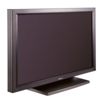
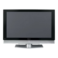
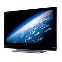
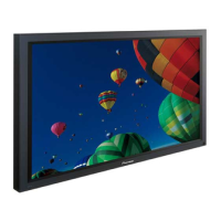
PDP-433CMX
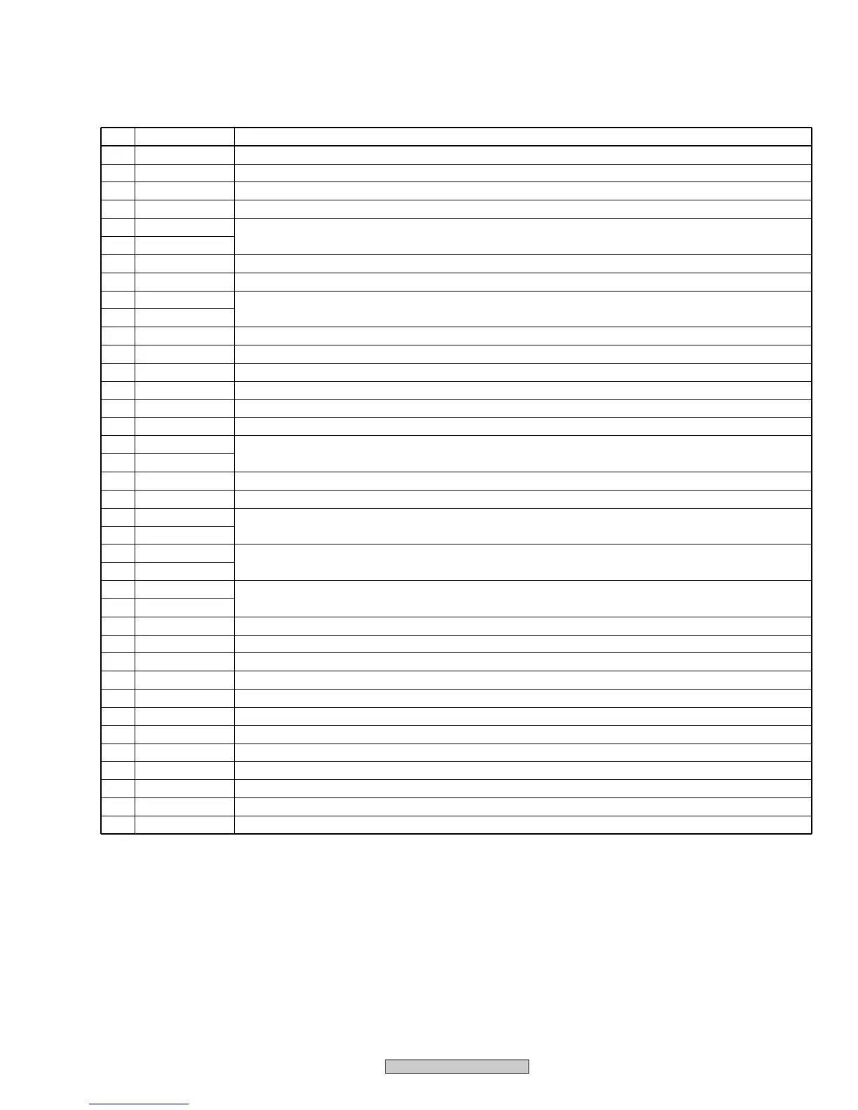
No. Pin Name Function
91 RDB Reading of external address space
92 HWRB Upper rank data (D15 to D8) writing of external address space
93 PLL_CE Chip enable signal output for AD/PLL
94 WAIT_IP WAIT input for IC102
95 NC
96 NC
Non connection
97 TXD_WU Communication data output (AD/PLL)
98 NC Non connection
99 VSS
100 VSS
GND
101 SCK_WU Communication clock input/output (AD/PLL)
102 WAIT_FLASH WAIT input for external flash memory
103 AVCC 3.3V power supply
104 VREF A/D and D/A reference voltage input
105 ULK_PLL PLL unlock signal input
106 EXT_FILM External film signal input
107 Not used
108 Not used
Pull-up
109 ACL_PC ACL input for PC (A/D input)
110 Not used Pull-up
111 I N a _ 30
112 INb_30
NC
113 AVSS
114 VSS
GND
115 N C
116 N C
Non connection
117 HD_W Horizontal sync. signal
118 FI FILM mode detecting input
119 HI Horizontal sync. count input
120 FDET_IP System frequency detecting input
121 EMG_IP IC102 forced hardware through output
122 IP_KILL IC101 forced stop output
123 MD0 Wide microcomputer operation mode (mode 6 fixing) (0)
124 MD1 Wide microcomputer operation mode (mode 6 fixing) (1)
125 MD2 Wide microcomputer operation mode (mode 6 fixing) (2)
126 IC_RST Reset signal input for ASIC
127 CS_102 Chip select output for IC102
128 CS_101 Chip select output for IC101
 Loading...