PDP-5071PU
70
1234
1234
C
D
F
A
B
E
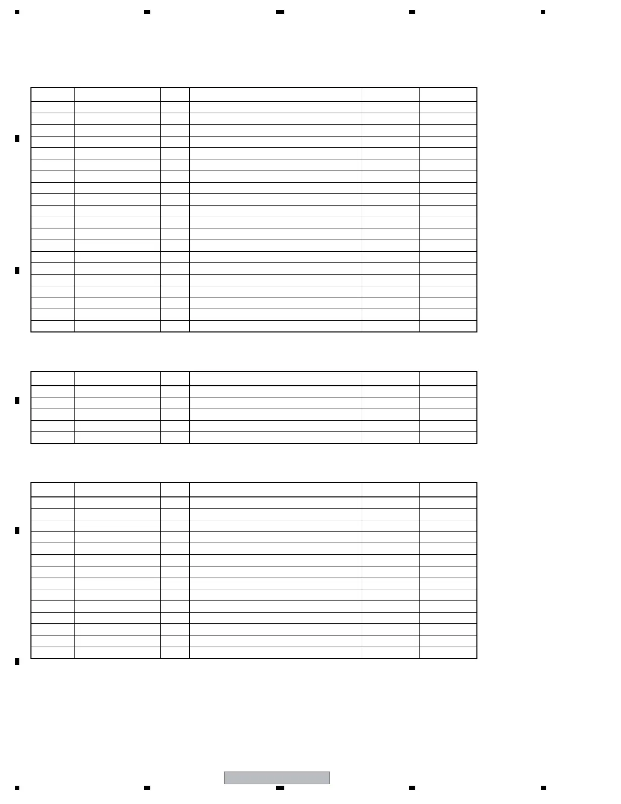
CN3002 (D12) ↔ Reserve (Non connection)
CN3151 (D24) ↔ SENSOR ASSY CN3651 (TE1)
Pin No. Pin Name I/O Function Voltage (V) TP
1
V+3V_D
O +3.3 V power supply output 3.3
2
V+3V_D
O +3.3 V power supply output 3.3
3
V+3V_D
O +3.3 V power supply output 3.3
–
–
–
–
–
–
–
–
–
–
–
–
–
–
–
–
–
–
–
–
–
–
–
–
–
–
–
–
–
–
–
–
–
4
GND_D
– GND
5
GND_D
– GND
6
GND_D
– GND
7
LED_R
O Red LED control output 0 to 3.3
8
LED_B
O Blue LED control output 0 to 3.3
9
MSEL
I Control select 0 to 3.3
10
PBF
I Panel type judge 0 to 3.3
11
NC
I Non connection
12
YOBI0
I Reserve input –
13
YOBI1
I Reserve input –
14
YOBI2
I Reserve input –
15
YOBI3
I Reserve input –
16
YOBI4
I Reserve input –
17 NC I Non connection
18 NC I Non connection
19
V+3V_STB
O STB 3.3 V power supply output 3.3
20
GND_D
– GND
Pin No. Pin Name I/O Function Voltage (V) TP
1
V+3.3V_EEP
O Power supply output for memory 3.3
2
E_SCL
O IIC communication clock signal 0 to 3.3
3
E_SDA
O IIC communication data signal 0 to 3.3
4
TEMP1
I Panel temperature sensor signal 0 to 3.3
5
GND
– GND
CN3601 (D21) ↔ POWER SUPPLY UNIT (P4)
Pin No. Pin Name I/O Function Voltage (V) TP
1
V+12V
I +12 V power supply input 12 –
2
V+12V
I +12 V power supply input 12 –
3
GND
– GND – –
4
GND
– GND – –
5
V+3.3V_STB
I STB3.3 V power supply input 0 to 3.3 –
6
GND
– GND – –
7
M_SW_DET
I Mechanism switch detection signal input 0 to 3.3 –
8
EXT_PD
O Power down signal 0 to 3.3 –
9
VSUS_ADJ
O VSUS power supply adjustment signal 0 to 3.3 –
10
PS_PD
I Power supply PD signal 0 to 3.3 –
11
RELAY
O Relay control 0 to 3.3 –
12
DRF_B
O Large power supply ON/OFF control signal 0 to 3.3 –
13
AC_DET
I AC power supply state input 0 to 3.3 –
14
PD_TRG_B
I Power down trigger signal 0 to 3.3 –
 Loading...