R10
1.-1
470
3
C9
C10
T
33
T
33
j)
2
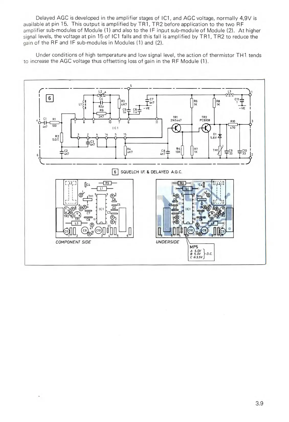
Delayed AGC is developed in the amplifier stages of IC1, and AGC voltage, normally 4,9V is
available at pin 15. This output is amplified by TR1, TR2 before application to the two RF
amplifier sub-modules of Module (1) and also to the IF input sub-module of Module (2). At higher
signal levels, the voltage at pin 15 of IC1 falls and this fall is amplified by TR1, TR2 to reduce the
gain of the RF and IF sub-modules in Modules (1) and (2).
Under conditions of high temperature and low signal level, the action of thermistor TH1 tends
to increase the AGC voltage thus offsetting loss of gain in the RF Module (1).
L2
5
L3
C7
R3
4K7
t
-
1
4
^
7
C5
C6-1- -VE
In
1n7
R8
C11
1K
-VE
TR2
PCB108
Cl
RI
0-1H
4n7
100
R2
5.0.11
1
1
0
11
'
C
l
3
2
4
14
5
15
.—C)—(
1
-
C3
74n7
R6
1K
TRI
2N5447
RS
R7
10K
1K
0
R4
4K7
DI
5.6V
T1-11
C8
— C2
6
T"'
0
4n7
T
ri
SQUELCH LE & DELAYED A.G.C.
4
-I R9
LI
I--
C7
TR2 5
c
TR1
C8
15
L3
6
0
COMPONENT SIDE
M P5
A 5.0V
B 5.0V
D.C.
C -43.5V
r
l
L2
J
1
1
1
1
L,
L. -
I
L 2
r
I
I
I
r
3.9