C3
T
1
22
R8
IM
R11
1K
R17
100
C8
—VE
TR4
MPSA13
TR3
PBC108B
R15
R16
68K
C9
39K
4n7
cit
lF
10
1
I
4
R18
3K9
—C7
— In
R14
CIO
—
100K
470p
—VE
C4
C5
2n2
2n2
R3
82K
R5
82K
R7
1—*
27K
100K
C6
1
150K
—H
I
2n2
R2
1K
C2
T1.70n
R6
33K
U
R9
1M
RIO
100K
TP1
n
NOISE LIMITER & HIGH & LOW PASS FILTER
COMPONENT SIDE
•
M P4
B 100mV
C 100mV
INJECT
40/nV P D AT 1kHz
13
TR3 b
C6
e 15
C10
G
ig.
'
6
16
TR1
TIS88A
Cl
n
0
—•
I I
'
n7
T
RI
1M
TR2
PBC108B
R12
R13
R4
f
33K
I
I
II
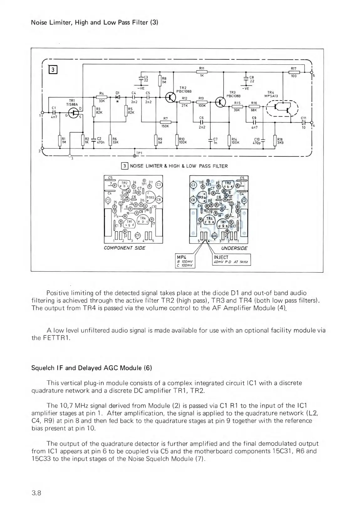
Noise Limiter, High and Low Pass Filter (3)
Positive limiting of the detected signal takes place at the diode D1 and out-of band audio
filtering is achieved through the active Miter TR2 (high pass), TR3 and TR4 (both low pass filters).
The output from TR4 is passed via the volume control to the AF Amplifier Module (4).
A low level unfiltered audio signal is made available for use with an optional facility module via
the FETTR1.
Squelch IF and Delayed AGC Module (6)
This vertical plug-in module consists of a complex integrated circuit ICI with a discrete
quadrature network and a discrete DC amplifier TR1, TR2.
The 10,7 MHz signal derived from Module (2) is passed via C1 R1 to the input of the IC1
amplifier stages at pin 1. After amplification, the signal is applied to the quadrature network (L2,
C4, R9) at pin 8 and then fed back to the quadrature stages at pin 9 together with the reference
bias present at pin 10.
The output of the quadrature detector is further amplified and the final demodulated output
from IC1 appears at pin 6 to be coupled via C5 and the motherboard components 15C31, R6 and
15C33 to the input stages of the Noise Squelch Module (7).
3.8