Internal Clock Source (S08ICSV3)
MC9S08QE128 MCU Series Reference Manual, Rev. 2
Freescale Semiconductor 211
r
3-2
CLKST
Clock Mode Status — The CLKST bits indicate the current clock mode. The CLKST bits don’t update
immediately after a write to the CLKS bits due to internal synchronization between clock domains.
00 Output of FLL is selected.
01 FLL Bypassed, Internal reference clock is selected.
10 FLL Bypassed, External reference clock is selected.
11 Reserved.
1
OSCINIT
OSC Initialization — If the external reference clock is selected by ERCLKEN or by the ICS being in FEE, FBE,
or FBELP mode, and if EREFS is set, then this bit is set after the initialization cycles of the external oscillator
clock have completed. This bit is only cleared when either ERCLKEN or EREFS are cleared.
0
FTRIM
ICS Fine Trim — The FTRIM bit controls the smallest adjustment of the internal reference clock frequency.
Setting FTRIM will increase the period and clearing FTRIM will decrease the period by the smallest amount
possible.
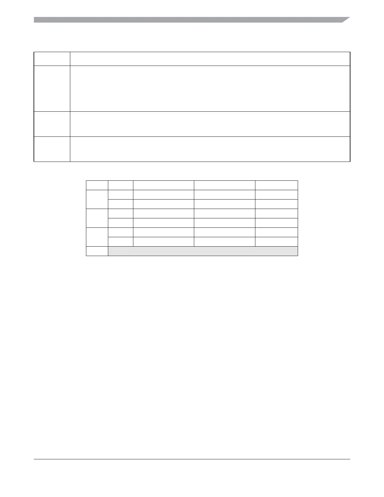
Table 11-7. DCO frequency range
1
1
The resulting bus clock frequency should not exceed the maximum specified bus
clock frequency of the device.
DRS DMX32 Reference range FLL factor DCO range
00
0 31.25 - 39.0625 kHz 512 16 - 20 Mhz
1 32.768 kHz 608 19.92 Mhz
01
0 31.25 - 39.0625 kHz 1024 32 - 40 Mhz
1 32.768 kHz 1216 39.85 Mhz
10
0 31.25 - 39.0625 kHz 1536 48 - 60 Mhz
1 32.768 kHz 1824 59.77 Mhz
11
Reserved
Table 11-6. ICS Status and Control Register Field Descriptions (continued)
Field Description