Chapter 18 Debug Module (DBG) (128K)
MC9S08QE128 MCU Series Reference Manual, Rev. 2
322 Freescale Semiconductor
• Ability to End-trace until reset and Begin-trace from reset
18.1.2 Modes of Operation
The on-chip ICE system can be enabled in all MCU functional modes. The DBG module is disabled if the
MCU is secure. The DBG module comparators are disabled when executing a Background Debug Mode
(BDM) command.
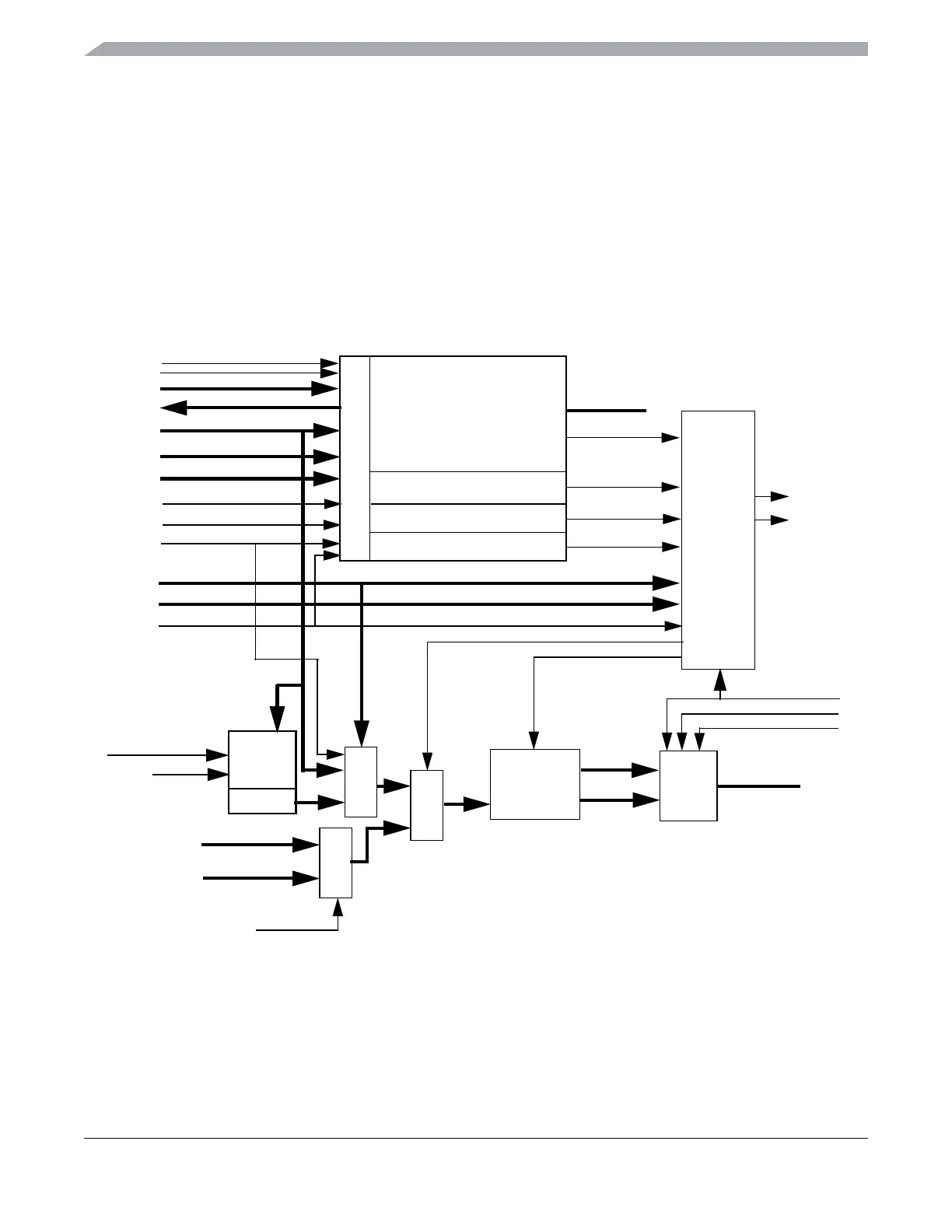
18.1.3 Block Diagram
Figure 18-1 shows the structure of the DBG module.
Figure 18-1. DBG Block Diagram
18.2 Signal Description
The DBG module contains no external signals.
mmu_ppage_sel
1
Comparator A
Address/Data/Control Registers
Tag
Force
Address Bus[16:0]
1
match_A
control
Read Data Bus
Read/Write
store
m
u
x
FIFO Data
ppage_sel
1
MCU in BDM
Change of Flow Indicators
subtract 2
m
u
x
Read DBGFH
Read DBGFL
register
Instr. Lastcycle
Bus Clk
Comparator B
match_B
8 deep
FIFO
m
u
x
event only
Write Data Bus
Trigger
Break
Control
Logic
c
o
n
t
r
o
FIFO Data
DBG Read Data Bus
DBG Module Enable
addr[16:0]
1
m
u
x
Write Data Bus
Read Data Bus
Read/Write
l
Comparator C
match_C
MCU reset
core_cof[1:0]
Read DBGFX
1. In 64K versions of this module there are only 16 address lines [15:0], there are no core_cpu_aob_14_t2,
core_cpu_aob_15_t2, core_ppage_t2[2:0], and ppage_sel signals.
core_cpu_aob_15_t2
1
core_ppage_t2[2:0]
1