Serial Peripheral Interface (S08SPIV3)
MC9S08QE128 MCU Series Reference Manual, Rev. 2
274 Freescale Semiconductor
NOTE
Ensure that the SPI should not be disabled (SPE=0) at the same time as a bit change to the CPHA bit. These
changes should be performed as separate operations or unexpected behavior may occur.
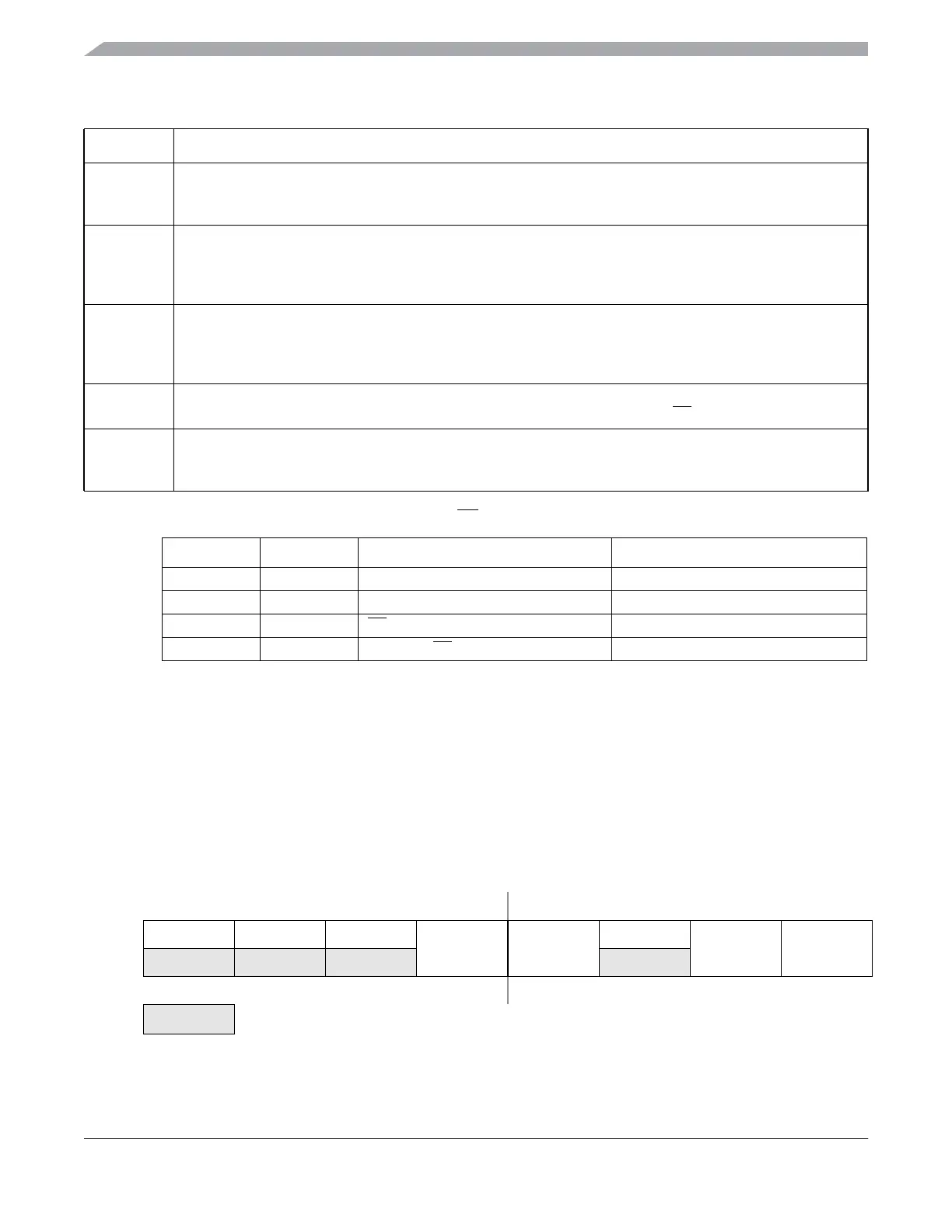
15.4.2 SPI Control Register 2 (SPIxC2)
This read/write register is used to control optional features of the SPI system. Bits 7, 6, 5, and 2 are not
implemented and always read 0.
4
MSTR
Master/Slave Mode Select
0 SPI module configured as a slave SPI device
1 SPI module configured as a master SPI device
3
CPOL
Clock Polarity — This bit effectively places an inverter in series with the clock signal from a master SPI or to a
slave SPI device. Refer to Section 15.5.1, “SPI Clock Formats” for more details.
0 Active-high SPI clock (idles low)
1 Active-low SPI clock (idles high)
2
CPHA
Clock Phase — This bit selects one of two clock formats for different kinds of synchronous serial peripheral
devices. Refer to Section 15.5.1, “SPI Clock Formats” for more details.
0 First edge on SPSCK occurs at the middle of the first cycle of an 8-cycle data transfer
1 First edge on SPSCK occurs at the start of the first cycle of an 8-cycle data transfer
1
SSOE
Slave Select Output Enable — This bit is used in combination with the mode fault enable (MODFEN) bit in
SPCR2 and the master/slave (MSTR) control bit to determine the function of the
SS pin as shown in Table 15-2.
0
LSBFE
LSB First (Shifter Direction)
0 SPI serial data transfers start with most significant bit
1 SPI serial data transfers start with least significant bit
Table 15-2. SS Pin Function
MODFEN SSOE Master Mode Slave Mode
0 0 General-purpose I/O (not SPI) Slave select input
0 1 General-purpose I/O (not SPI) Slave select input
10
SS input for mode fault Slave select input
1 1 Automatic
SS output Slave select input
76543210
R000
MODFEN BIDIROE
0
SPISWAI SPC0
W
Reset 00000000
= Unimplemented or Reserved
Figure 15-6. SPI Control Register 2 (SPIxC2)
Table 15-1. SPIxC1 Field Descriptions (continued)
Field Description